Carbon nanotube
From Wikipedia, the free encyclopedia
Not to be confused with Carbon fiber.
| Part of a series of articles on |
| Nanomaterials |
|---|
| Fullerenes |
| Nanoparticles |
| Nanotechnology portal' |

Rotating Carbon Nanotube
Nanotubes are members of the fullerene structural family. Their name is derived from their long, hollow structure with the walls formed by one-atom-thick sheets of carbon, called graphene. These sheets are rolled at specific and discrete ("chiral") angles, and the combination of the rolling angle and radius decides the nanotube properties; for example, whether the individual nanotube shell is a metal or semiconductor. Nanotubes are categorized as single-walled nanotubes (SWNTs) and multi-walled nanotubes (MWNTs). Individual nanotubes naturally align themselves into "ropes" held together by van der Waals forces, more specifically, pi-stacking.
Applied quantum chemistry, specifically, orbital hybridization best describes chemical bonding in nanotubes. The chemical bonding of nanotubes is composed entirely of sp2 bonds, similar to those of graphite. These bonds, which are stronger than the sp3 bonds found in alkanes and diamond, provide nanotubes with their unique strength.
Contents
[hide]- 1 Types of carbon nanotubes and related structures
- 2 Properties
- 3 Synthesis
- 4 Current applications
- 5 Potential applications
- 6 Discovery
- 7 See also
- 8 References
- 9 External links
[edit]
Terminology[edit]
There is no consensus on some terms describing carbon nanotubes in scientific literature: both "-wall" and "-walled" are being used in combination with "single", "double", "triple" or "multi", and the letter C is often omitted in the abbreviation; for example, multi-walled carbon nanotube (MWNT).Single-walled[edit]
 Armchair (n,n) i.e.: m=n
 The translation vector is bent, while the chiral vector stays straight
 Graphene nanoribbon
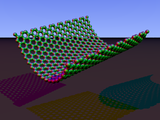 The chiral vector is bent, while the translation vector stays straight
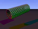 Zigzag (n,0)
 Chiral (n,m)
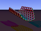 n and m can be counted at the end of the tube
 Graphene nanoribbon


SWNTs are an important variety of carbon nanotube because most of their properties change significantly with the (n,m) values, and this dependence is non-monotonic (see Kataura plot). In particular, their band gap can vary from zero to about 2 eV and their electrical conductivity can show metallic or semiconducting behavior. Single-walled nanotubes are likely candidates for miniaturizing electronics. The most basic building block of these systems is the electric wire, and SWNTs with diameters of an order of a nanometer can be excellent conductors.[3][4] One useful application of SWNTs is in the development of the first intermolecular field-effect transistors (FET). The first intermolecular logic gate using SWCNT FETs was made in 2001.[5] A logic gate requires both a p-FET and an n-FET. Because SWNTs are p-FETs when exposed to oxygen and n-FETs otherwise, it is possible to protect half of an SWNT from oxygen exposure, while exposing the other half to oxygen. This results in a single SWNT that acts as a NOT logic gate with both p and n-type FETs within the same molecule.
Single-walled nanotubes are dropping precipitously in price, from around $1500 per gram as of 2000 to retail prices of around $50 per gram of as-produced 40–60% by weight SWNTs as of March 2010.[citation needed]
Multi-walled[edit]


Double-walled carbon nanotubes (DWNT) form a special class of nanotubes because their morphology and properties are similar to those of SWNT but their resistance to chemicals is significantly improved. This is especially important when functionalization is required (this means grafting of chemical functions at the surface of the nanotubes) to add new properties to the CNT. In the case of SWNT, covalent functionalization will break some C=C double bonds, leaving "holes" in the structure on the nanotube and, thus, modifying both its mechanical and electrical properties. In the case of DWNT, only the outer wall is modified. DWNT synthesis on the gram-scale was first proposed in 2003[6] by the CCVD technique, from the selective reduction of oxide solutions in methane and hydrogen.
The telescopic motion ability of inner shells[7] and their unique mechanical properties[8] will permit the use of multi-walled nanotubes as main movable arms in coming nanomechanical devices. Retraction force that occurs to telescopic motion caused by the Lennard-Jones interaction between shells and its value is about 1.5 nN.[9]
Torus[edit]

Nanobud[edit]
Carbon nanobuds are a newly created material combining two previously discovered allotropes of carbon: carbon nanotubes and fullerenes. In this new material, fullerene-like "buds" are covalently bonded to the outer sidewalls of the underlying carbon nanotube. This hybrid material has useful properties of both fullerenes and carbon nanotubes. In particular, they have been found to be exceptionally good field emitters. In composite materials, the attached fullerene molecules may function as molecular anchors preventing slipping of the nanotubes, thus improving the composite’s mechanical properties.Graphenated carbon nanotubes (g-CNTs)[edit]

The fundamental advantage of an integrated graphene-CNT structure is the high surface area three-dimensional framework of the CNTs coupled with the high edge density of graphene. Graphene edges provide significantly higher charge density and reactivity than the basal plane, but they are difficult to arrange in a three-dimensional, high volume-density geometry. CNTs are readily aligned in a high density geometry (i.e., a vertically aligned forest)[16] but lack high charge density surfaces—the sidewalls of the CNTs are similar to the basal plane of graphene and exhibit low charge density except where edge defects exist. Depositing a high density of graphene foliates along the length of aligned CNTs can significantly increase the total charge capacity per unit of nominal area as compared to other carbon nanostructures.[17]
Nitrogen Doped Carbon Nanotubes[edit]
Nitrogen doped carbon nanotubes (N-CNT's), can be produced through 5 main methods, Chemical Vapor Deposition,[18][19] high-temperature and high-pressure reactions, gas-solid reaction of amorphous carbon with NH3 at high temperature,[20] solid reaction,[21] and solvothermal synthesis.[22]N-CNTs can also be prepared by a CVD method of pyrolysizing melamine under Ar at elevated temperatures of 800oC - 980oC. However synthesis via CVD and melamine results in the formation of bamboo structured CNTs. XPS spectra of grown N-CNT's reveals nitrogen in five main components, pyridinic nitrogen, pyrrolic nitrogen, quaternary nitrogen, and nitrogen oxides. Furthermore synthesis temperature affects the type of nitrogen configuration.[23]
Nitrogen doping plays a pivotal role in Lithium storage. N-doping provides defects in the walls of CNT's allowing for Li ions to diffuse into interwall space. It also increases capacity by providing more favorable bind of N-doped sites. N-CNT's are also much more reactive to metal oxide nanoparticle deposition which can further enhance storage capacity, especially in anode materials for Li-ion batteries.[24] However Boron doped nanotubes have been shown to make batteries with triple capacity.[25]
Peapod[edit]
A Carbon peapod[26][27] is a novel hybrid carbon material which traps fullerene inside a carbon nanotube. It can possess interesting magnetic properties with heating and irradiating. It can also be applied as an oscillator during theoretical investigations and predictions.[28][29]Cup-stacked carbon nanotubes[edit]
Cup-stacked carbon nanotubes (CSCNTs) differ from other quasi-1D carbon structures, which normally behave as quasi-metallic conductors of electrons. CSCNTs exhibit semiconducting behaviors due to the stacking microstructure of graphene layers.[30]Extreme carbon nanotubes[edit]

The shortest carbon nanotube is the organic compound cycloparaphenylene, which was synthesized in early 2009.[31][32]
The thinnest carbon nanotube is armchair (2,2) CNT with a diameter of 3 Å. This nanotube was grown inside a multi-walled carbon nanotube. Assigning of carbon nanotube type was done by combination of high-resolution transmission electron microscopy (HRTEM), Raman spectroscopy and density functional theory (DFT) calculations.[33]
The thinnest freestanding single-walled carbon nanotube is about 4.3 Å in diameter. Researchers suggested that it can be either (5,1) or (4,2) SWCNT, but exact type of carbon nanotube remains questionable.[34] (3,3), (4,3) and (5,1) carbon nanotubes (all about 4 Å in diameter) were unambiguously identified using aberration-corrected high-resolution transmission electron microscopy inside double-walled CNTs.[35]
The highest density of CNTs was achieved in 2013, grown on a conductive titanium-coated copper surface that was coated with co-catalysts cobalt and molybdenum at lower than typical temperatures of 450 °C. The tubes averaged a height of 0.38 μm and a mass density of 1.6 g cm−3. The material showed ohmic conductivity (lowest resistance ∼22 kΩ).[36][37]
Properties[edit]
Strength[edit]
Carbon nanotubes are the strongest and stiffest materials yet discovered in terms of tensile strength and elastic modulus respectively. This strength results from the covalent sp2 bonds formed between the individual carbon atoms. In 2000, a multi-walled carbon nanotube was tested to have a tensile strength of 63 gigapascals (GPa).[38] (For illustration, this translates into the ability to endure tension of a weight equivalent to 6422 kg (14,158 lbs) on a cable with cross-section of 1 mm2.) Further studies, such as one conducted in 2008, revealed that individual CNT shells have strengths of up to ~100 GPa, which is in agreement with quantum/atomistic models.[39] Since carbon nanotubes have a low density for a solid of 1.3 to 1.4 g/cm3,[40] its specific strength of up to 48,000 kN·m·kg−1 is the best of known materials, compared to high-carbon steel's 154 kN·m·kg−1.Under excessive tensile strain, the tubes will undergo plastic deformation, which means the deformation is permanent. This deformation begins at strains of approximately 5% and can increase the maximum strain the tubes undergo before fracture by releasing strain energy.
Although the strength of individual CNT shells is extremely high, weak shear interactions between adjacent shells and tubes leads to significant reductions in the effective strength of multi-walled carbon nanotubes and carbon nanotube bundles down to only a few GPa’s.[41] This limitation has been recently addressed by applying high-energy electron irradiation, which crosslinks inner shells and tubes, and effectively increases the strength of these materials to ~60 GPa for multi-walled carbon nanotubes[39] and ~17 GPa for double-walled carbon nanotube bundles.[41]
CNTs are not nearly as strong under compression. Because of their hollow structure and high aspect ratio, they tend to undergo buckling when placed under compressive, torsional, or bending stress.[42]
| Material | Young's modulus (TPa) | Tensile strength (GPa) | Elongation at break (%) |
|---|---|---|---|
| SWNTE | ~1 (from 1 to 5) | 13–53 | 16 |
| Armchair SWNTT | 0.94 | 126.2 | 23.1 |
| Zigzag SWNTT | 0.94 | 94.5 | 15.6–17.5 |
| Chiral SWNT | 0.92 | ||
| MWNTE | 0.2[38]–0.8[47]–0.95[38] | 11[38]–63[38]–150[47] | |
| Stainless steelE | 0.186[48]–0.214[49] | 0.38[48]–1.55[49] | 15–50 |
| Kevlar–29&149E | 0.06–0.18[50] | 3.6–3.8[50] | ~2 |
The above discussion referred to axial properties of the nanotube, whereas simple geometrical considerations suggest that carbon nanotubes should be much softer in the radial direction than along the tube axis. Indeed, TEM observation of radial elasticity suggested that even the van der Waals forces can deform two adjacent nanotubes.[51] Nanoindentation experiments, performed by several groups on multiwalled carbon nanotubes[52][53] and tapping/contact mode atomic force microscope measurement performed on single-walled carbon nanotube,[54] indicated Young's modulus of the order of several GPa confirming that CNTs are indeed rather soft in the radial direction.
Hardness[edit]
Standard single-walled carbon nanotubes can withstand a pressure up to 25 GPa without deformation. They then undergo a transformation to superhard phase nanotubes. Maximum pressures measured using current experimental techniques are around 55 GPa. However, these new superhard phase nanotubes collapse at an even higher, albeit unknown, pressure.The bulk modulus of superhard phase nanotubes is 462 to 546 GPa, even higher than that of diamond (420 GPa for single diamond crystal).[55]
Kinetic properties[edit]
Multi-walled nanotubes are multiple concentric nanotubes precisely nested within one another. These exhibit a striking telescoping property whereby an inner nanotube core may slide, almost without friction, within its outer nanotube shell, thus creating an atomically perfect linear or rotational bearing. This is one of the first true examples of molecular nanotechnology, the precise positioning of atoms to create useful machines. Already, this property has been utilized to create the world's smallest rotational motor.[56] Future applications such as a gigahertz mechanical oscillator are also envisioned.Electrical properties[edit]

However, this rule has exceptions, because curvature effects in small diameter carbon nanotubes can strongly influence electrical properties. Thus, a (5,0) SWCNT that should be semiconducting in fact is metallic according to the calculations. Likewise, vice versa—zigzag and chiral SWCNTs with small diameters that should be metallic have finite gap (armchair nanotubes remain metallic).[57] In theory, metallic nanotubes can carry an electric current density of 4 × 10⁹ A/cm2, which is more than 1,000 times greater than those of metals such as copper,[58] where for copper interconnects current densities are limited by electromigration.
Because of their nanoscale cross-section, electrons propagate only along the tube's axis and electron transport involves quantum effects. As a result, carbon nanotubes are frequently referred to as one-dimensional conductors. The maximum electrical conductance of a single-walled carbon nanotube is 2G0, where G0 = 2e2/h is the conductance of a single ballistic quantum channel.[59]
There have been reports of intrinsic superconductivity in carbon nanotubes.[60][61][62] Many other experiments, however, found no evidence of superconductivity, and the validity of these claims of intrinsic superconductivity remains a subject of debate.[63]
Optical properties[edit]
Main article: Optical properties of carbon nanotubes
Thermal properties[edit]
Main article: Thermal properties of nanostructures
All nanotubes are expected to be very good thermal conductors along the tube, exhibiting a property known as "ballistic conduction", but good insulators laterally to the tube axis. Measurements show that a SWNT has a room-temperature thermal conductivity along its axis of about 3500 W·m−1·K−1;[64] compare this to copper, a metal well known for its good thermal conductivity, which transmits 385 W·m−1·K−1. A SWNT has a room-temperature thermal conductivity across its axis (in the radial direction) of about 1.52 W·m−1·K−1,[65] which is about as thermally conductive as soil. The temperature stability of carbon nanotubes is estimated to be up to 2800 °C in vacuum and about 750 °C in air.[66]Defects[edit]
As with any material, the existence of a crystallographic defect affects the material properties. Defects can occur in the form of atomic vacancies. High levels of such defects can lower the tensile strength by up to 85%. An important example is the Stone Wales defect, which creates a pentagon and heptagon pair by rearrangement of the bonds. Because of the very small structure of CNTs, the tensile strength of the tube is dependent on its weakest segment in a similar manner to a chain, where the strength of the weakest link becomes the maximum strength of the chain.Crystallographic defects also affect the tube's electrical properties. A common result is lowered conductivity through the defective region of the tube. A defect in armchair-type tubes (which can conduct electricity) can cause the surrounding region to become semiconducting, and single monatomic vacancies induce magnetic properties.[67]
Crystallographic defects strongly affect the tube's thermal properties. Such defects lead to phonon scattering, which in turn increases the relaxation rate of the phonons. This reduces the mean free path and reduces the thermal conductivity of nanotube structures. Phonon transport simulations indicate that substitutional defects such as nitrogen or boron will primarily lead to scattering of high-frequency optical phonons. However, larger-scale defects such as Stone Wales defects cause phonon scattering over a wide range of frequencies, leading to a greater reduction in thermal conductivity.[68]
Toxicity[edit]
See also: Fullerene#Safety and toxicity
The toxicity of carbon nanotubes has been an important question in nanotechnology. As of 2007, such research has just begun. The data are still fragmentary and subject to criticism. Preliminary results highlight the difficulties in evaluating the toxicity of this heterogeneous material. Parameters such as structure, size distribution, surface area, surface chemistry, surface charge, and agglomeration state as well as purity of the samples, have considerable impact on the reactivity of carbon nanotubes. However, available data clearly show that, under some conditions, nanotubes can cross membrane barriers, which suggests that, if raw materials reach the organs, they can induce harmful effects such as inflammatory and fibrotic reactions.[69]Under certain conditions CNTs can enter human cells and accumulate in the cytoplasm, causing cell death.[70]
Results of rodent studies collectively show that regardless of the process by which CNTs were synthesized and the types and amounts of metals they contained, CNTs were capable of producing inflammation, epithelioid granulomas (microscopic nodules), fibrosis, and biochemical/toxicological changes in the lungs.[71] Comparative toxicity studies in which mice were given equal weights of test materials showed that SWCNTs were more toxic than quartz, which is considered a serious occupational health hazard when chronically inhaled. As a control, ultrafine carbon black was shown to produce minimal lung responses.[72]
Carbon nano tubes deposit in the alveolar ducts by aligning length wise with the airways; the nano tubes will often combine with metals. [73] The needle-like fiber shape of CNTs is similar to asbestos fibers. This raises the idea that widespread use of carbon nanotubes may lead to pleural mesothelioma, a cancer of the lining of the lungs or peritoneal mesothelioma, a cancer of the lining of the abdomen (both caused by exposure to asbestos). A recently published pilot study supports this prediction.[74] Scientists exposed the mesothelial lining of the body cavity of mice to long multiwalled carbon nanotubes and observed asbestos-like, length-dependent, pathogenic behavior that included inflammation and formation of lesions known as granulomas. Authors of the study conclude:
This is of considerable importance, because research and business communities continue to invest heavily in carbon nanotubes for a wide range of products under the assumption that they are no more hazardous than graphite. Our results suggest the need for further research and great caution before introducing such products into the market if long-term harm is to be avoided.[74]Although further research is required, the available data suggests that under certain conditions, especially those involving chronic exposure, carbon nanotubes can pose a serious risk to human health.[69][70][72][74]
Synthesis[edit]

Arc discharge[edit]
Nanotubes were observed in 1991 in the carbon soot of graphite electrodes during an arc discharge, by using a current of 100 amps, that was intended to produce fullerenes.[75] However the first macroscopic production of carbon nanotubes was made in 1992 by two researchers at NEC's Fundamental Research Laboratory.[76] The method used was the same as in 1991. During this process, the carbon contained in the negative electrode sublimates because of the high-discharge temperatures. Because nanotubes were initially discovered using this technique, it has been the most widely used method of nanotube synthesis.The yield for this method is up to 30% by weight and it produces both single- and multi-walled nanotubes with lengths of up to 50 micrometers with few structural defects.[40]
Laser ablation[edit]
In laser ablation, a pulsed laser vaporizes a graphite target in a high-temperature reactor while an inert gas is bled into the chamber. Nanotubes develop on the cooler surfaces of the reactor as the vaporized carbon condenses. A water-cooled surface may be included in the system to collect the nanotubes.This process was developed by Dr. Richard Smalley and co-workers at Rice University, who at the time of the discovery of carbon nanotubes, were blasting metals with a laser to produce various metal molecules. When they heard of the existence of nanotubes they replaced the metals with graphite to create multi-walled carbon nanotubes.[77] Later that year the team used a composite of graphite and metal catalyst particles (the best yield was from a cobalt and nickel mixture) to synthesize single-walled carbon nanotubes.[78]
The laser ablation method yields around 70% and produces primarily single-walled carbon nanotubes with a controllable diameter determined by the reaction temperature. However, it is more expensive than either arc discharge or chemical vapor deposition.[40]
Plasma torch[edit]
Single-walled carbon nanotubes can be synthesized by the induction thermal plasma method, discovered in 2005 by groups from the University of Sherbrooke and the National Research Council of Canada.[79] The method is similar to arc-discharge in that both use ionized gas to reach the high temperature necessary to vaporize carbon-containing substances and the metal catalysts necessary for the ensuing nanotube growth. The thermal plasma is induced by high frequency oscillating currents in a coil, and is maintained in flowing inert gas. Typically, a feedstock of carbon black and metal catalyst particles is fed into the plasma, and then cooled down to form single-walled carbon nanotubes. Different single-wall carbon nanotube diameter distributions can be synthesized.The induction thermal plasma method can produce up to 2 grams of nanotube material per minute, which is higher than the arc-discharge or the laser ablation methods.
Chemical vapor deposition (CVD)[edit]

During CVD, a substrate is prepared with a layer of metal catalyst particles, most commonly nickel, cobalt,[84] iron, or a combination.[85] The metal nanoparticles can also be produced by other ways, including reduction of oxides or oxides solid solutions. The diameters of the nanotubes that are to be grown are related to the size of the metal particles. This can be controlled by patterned (or masked) deposition of the metal, annealing, or by plasma etching of a metal layer. The substrate is heated to approximately 700°C. To initiate the growth of nanotubes, two gases are bled into the reactor: a process gas (such as ammonia, nitrogen or hydrogen) and a carbon-containing gas (such as acetylene, ethylene, ethanol or methane). Nanotubes grow at the sites of the metal catalyst; the carbon-containing gas is broken apart at the surface of the catalyst particle, and the carbon is transported to the edges of the particle, where it forms the nanotubes. This mechanism is still being studied.[86] The catalyst particles can stay at the tips of the growing nanotube during growth, or remain at the nanotube base, depending on the adhesion between the catalyst particle and the substrate.[87] Thermal catalytic decomposition of hydrocarbon has become an active area of research and can be a promising route for the bulk production of CNTs. Fluidised bed reactor is the most widely used reactor for CNT preparation. Scale-up of the reactor is the major challenge.[88][89]
CVD is a common method for the commercial production of carbon nanotubes. For this purpose, the metal nanoparticles are mixed with a catalyst support such as MgO or Al2O3 to increase the surface area for higher yield of the catalytic reaction of the carbon feedstock with the metal particles. One issue in this synthesis route is the removal of the catalyst support via an acid treatment, which sometimes could destroy the original structure of the carbon nanotubes. However, alternative catalyst supports that are soluble in water have proven effective for nanotube growth.[90]
If a plasma is generated by the application of a strong electric field during growth (plasma-enhanced chemical vapor deposition), then the nanotube growth will follow the direction of the electric field.[91] By adjusting the geometry of the reactor it is possible to synthesize vertically aligned carbon nanotubes[92] (i.e., perpendicular to the substrate), a morphology that has been of interest to researchers interested in the electron emission from nanotubes. Without the plasma, the resulting nanotubes are often randomly oriented. Under certain reaction conditions, even in the absence of a plasma, closely spaced nanotubes will maintain a vertical growth direction resulting in a dense array of tubes resembling a carpet or forest.
Of the various means for nanotube synthesis, CVD shows the most promise for industrial-scale deposition, because of its price/unit ratio, and because CVD is capable of growing nanotubes directly on a desired substrate, whereas the nanotubes must be collected in the other growth techniques. The growth sites are controllable by careful deposition of the catalyst.[93] In 2007, a team from Meijo University demonstrated a high-efficiency CVD technique for growing carbon nanotubes from camphor.[94] Researchers at Rice University, until recently led by the late Richard Smalley, have concentrated upon finding methods to produce large, pure amounts of particular types of nanotubes. Their approach grows long fibers from many small seeds cut from a single nanotube; all of the resulting fibers were found to be of the same diameter as the original nanotube and are expected to be of the same type as the original nanotube.[95]
Super-growth CVD[edit]
Super-growth CVD (water-assisted chemical vapor deposition) was developed by Kenji Hata, Sumio Iijima and co-workers at AIST, Japan.[96] In this process, the activity and lifetime of the catalyst are enhanced by addition of water into the CVD reactor. Dense millimeter-tall nanotube "forests", aligned normal to the substrate, were produced. The forests growth rate could be expressed, as
 is the characteristic catalyst lifetime.[97]
Their specific surface exceeds 1,000 m2/g (capped) or 2,200 m2/g (uncapped),[98] surpassing the value of 400–1,000 m2/g for HiPco samples. The synthesis efficiency is about 100 times higher than for the laser ablation method. The time required to make SWNT forests of the height of 2.5 mm by this method was 10 minutes in 2004. Those SWNT forests can be easily separated from the catalyst, yielding clean SWNT material (purity >99.98%) without further purification. For comparison, the as-grown HiPco CNTs contain about 5–35%[99] of metal impurities; it is therefore purified through dispersion and centrifugation that damages the nanotubes. Super-growth avoids this problem. Patterned highly organized single-walled nanotube structures were successfully fabricated using the super-growth technique.
The mass density of super-growth CNTs is about 0.037 g/cm3.[100][101] It is much lower than that of conventional CNT powders (~1.34 g/cm3), probably because the latter contain metals and amorphous carbon.
The super-growth method is basically a variation of CVD. Therefore, it is possible to grow material containing SWNT, DWNTs and MWNTs, and to alter their ratios by tuning the growth conditions.[102] Their ratios change by the thinness of the catalyst. Many MWNTs are included so that the diameter of the tube is wide.[101]
The vertically aligned nanotube forests originate from a "zipping effect" when they are immersed in a solvent and dried. The zipping effect is caused by the surface tension of the solvent and the van der Waals forces between the carbon nanotubes. It aligns the nanotubes into a dense material, which can be formed in various shapes, such as sheets and bars, by applying weak compression during the process. Densification increases the Vickers hardness by about 70 times and density is 0.55 g/cm3. The packed carbon nanotubes are more than 1 mm long and have a carbon purity of 99.9% or higher; they also retain the desirable alignment properties of the nanotubes forest.[103]
Natural, incidental, and controlled flame environments[edit]
Fullerenes and carbon nanotubes are not necessarily products of high-tech laboratories; they are commonly formed in such mundane places as ordinary flames,[104] produced by burning methane,[105] ethylene,[106] and benzene,[107] and they have been found in soot from both indoor and outdoor air.[108] However, these naturally occurring varieties can be highly irregular in size and quality because the environment in which they are produced is often highly uncontrolled. Thus, although they can be used in some applications, they can lack in the high degree of uniformity necessary to satisfy the many needs of both research and industry. Recent efforts have focused on producing more uniform carbon nanotubes in controlled flame environments.[109][110][111][112] Such methods have promise for large-scale, low-cost nanotube synthesis based on theoretical models,[113] though they must compete with rapidly developing large scale CVD production.Removal of catalysts[edit]
Nanoscale metal catalysts are important ingredients for fixed- and fluidized-bed CVD synthesis of CNTs. They allow increasing the growth efficiency of CNTs and may give control over their structure and chirality.[114] During synthesis, catalysts can convert carbon precursors into tubular carbon structures but can also form encapsulating carbon overcoats. Together with metal oxide supports they may therefore attach to or become incorporated into the CNT product.[115] The presence of metal impurities can be problematic for many applications. Especially catalyst metals like nickel, cobalt or yttrium may be of toxicological concern.[116] While un-encapsulated catalyst metals may be readily removable by acid washing, encapsulated ones require oxidative treatment for opening their carbon shell.[117] The effective removal of catalysts, especially of encapsulated ones, while preserving the CNT structure is a challenge and has been addressed in many studies.[118][119] A new approach to break carbonaceaous catalyst encapsulations is based on rapid thermal annealing.[120][edit]

In addition to separation of semiconducting and metallic SWNTs, it is possible to sort SWNTs by length, diameter, and chirality. The highest resolution length sorting, with length variation of <10%, has thus far been achieved by size exclusion chromatography (SEC) of DNA-dispersed carbon nanotubes (DNA-SWNT).[126] SWNT diameter separation has been achieved by density-gradient ultracentrifugation (DGU)[127] using surfactant-dispersed SWNTs and by ion-exchange chromatography (IEC) for DNA-SWNT.[128] Purification of individual chiralities has also been demonstrated with IEC of DNA-SWNT: specific short DNA oligomers can be used to isolate individual SWNT chiralities. Thus far, 12 chiralities have been isolated at purities ranging from 70% for (8,3) and (9,5) SWNTs to 90% for (6,5), (7,5) and (10,5)SWNTs.[129] There have been successful efforts to integrate these purified nanotubes into devices, e. g. FETs.[130]
An alternative to separation is development of a selective growth of semiconducting or metallic CNTs. Recently, a new CVD recipe that involves a combination of ethanol and methanol gases and quartz substrates resulting in horizontally aligned arrays of 95–98% semiconducting nanotubes was announced.[131]
Nanotubes are usually grown on nanoparticles of magnetic metal (Fe, Co), which facilitates production of electronic (spintronic) devices. In particular, control of current through a field-effect transistor by magnetic field has been demonstrated in such a single-tube nanostructure.[132]
Current applications[edit]
Current use and application of nanotubes has mostly been limited to the use of bulk nanotubes, which is a mass of rather unorganized fragments of nanotubes. Bulk nanotube materials may never achieve a tensile strength similar to that of individual tubes, but such composites may, nevertheless, yield strengths sufficient for many applications. Bulk carbon nanotubes have already been used as composite fibers in polymers to improve the mechanical, thermal and electrical properties of the bulk product.- Easton-Bell Sports, Inc. have been in partnership with Zyvex Performance Materials, using CNT technology in a number of their bicycle components—including flat and riser handlebars, cranks, forks, seatposts, stems and aero bars.
- Zyvex Technologies has also built a 54' maritime vessel, the Piranha Unmanned Surface Vessel, as a technology demonstrator for what is possible using CNT technology. CNTs help improve the structural performance of the vessel, resulting in a lightweight 8,000 lb boat that can carry a payload of 15,000 lb over a range of 2,500 miles.[133]
- Amroy Europe Oy manufactures Hybtonite carbon nanoepoxy resins where carbon nanotubes have been chemically activated to bond to epoxy, resulting in a composite material that is 20% to 30% stronger than other composite materials. It has been used for wind turbines, marine paints and variety of sports gear such as skis, ice hockey sticks, baseball bats, hunting arrows, and surfboards.[134]
- tips for atomic force microscope probes[135]
- in tissue engineering, carbon nanotubes can act as scaffolding for bone growth[136]
Potential applications[edit]
Main article: Potential applications of carbon nanotubes
The strength and flexibility of carbon nanotubes makes them of potential use in controlling other nanoscale structures, which suggests they will have an important role in nanotechnology engineering. The highest tensile strength of an individual multi-walled carbon nanotube has been tested to be is 63 GPa.[38] Carbon nanotubes were found in Damascus steel from the 17th century, possibly helping to account for the legendary strength of the swords made of it.[137][138]Structural[edit]
Because of the carbon nanotube's superior mechanical properties, many structures have been proposed ranging from everyday items like clothes and sports gear to combat jackets and space elevators.[139] However, the space elevator will require further efforts in refining carbon nanotube technology, as the practical tensile strength of carbon nanotubes can still be greatly improved.[40]For perspective, outstanding breakthroughs have already been made. Pioneering work led by Ray H. Baughman at the NanoTech Institute has shown that single and multi-walled nanotubes can produce materials with toughness unmatched in the man-made and natural worlds.[140][141]
Carbon nanotubes are also a promising material as building blocks in bio-mimetic hierarchical composite materials given their exceptional mechanical properties (~1 TPa in modulus, and ~100 GPa in strength). Initial attempts to incorporate CNTs into hierarchical structures led to mechanical properties that were significantly lower than these achievable limits. Windle et al. have used an in situ chemical vapor deposition (CVD) spinning method to produce continuous CNT yarns from CVD grown CNT aerogels.[142][143] With this technology, they fabricated CNT yarns with strengths as high as ~9 GPa at small gage lengths of ~1 mm, however, defects resulted in a reduction of specific strength to ~1 GPa at 20 mm gage length.[144][145] Espinosa et al. developed high performance DWNT-polymer composite yarns by twisting and stretching ribbons of randomly oriented bundles of DWNTs thinly coated with polymeric organic compounds. These DWNT-polymer yarns exhibited unusually high energy to failure of ~100 J·g−1 (comparable to one of the toughest natural materials – spider silk[146]), and strength as high as ~1.4 GPa.[147] Effort is ongoing to produce CNT composites that incorporate tougher matrix materials, such as Kevlar, to further improve on the mechanical properties toward those of individual CNTs.
Because of the high mechanical strength of carbon nanotubes, research is being made into weaving them into clothes to create stab-proof and bulletproof clothing. The nanotubes would effectively stop the bullet from penetrating the body, although the bullet's kinetic energy would likely cause broken bones and internal bleeding.[148]
Electrical circuits[edit]
Nanotube-based transistors, also known as carbon nanotube field-effect transistors (CNTFETs), have been made that operate at room temperature and that are capable of digital switching using a single electron.[149] However, one major obstacle to realization of nanotubes has been the lack of technology for mass production. In 2001 IBM researchers demonstrated how metallic nanotubes can be destroyed, leaving semiconducting ones behind for use as transistors. Their process is called "constructive destruction," which includes the automatic destruction of defective nanotubes on the wafer.[150] This process, however, only gives control over the electrical properties on a statistical scale.The potential of carbon nanotubes was demonstrated in 2003 when room-temperature ballistic transistors with ohmic metal contacts and high-k gate dielectric were reported, showing 20–30x higher ON current than state-of-the-art Si MOSFETs. This presented an important advance in the field as CNT was shown to potentially outperform Si. At the time, a major challenge was ohmic metal contact formation. In this regard, palladium, which is a high-work function metal was shown to exhibit Schottky barrier-free contacts to semiconducting nanotubes with diameters >1.7 nm.[151][152]
The first nanotube integrated memory circuit was made in 2004. One of the main challenges has been regulating the conductivity of nanotubes. Depending on subtle surface features a nanotube may act as a plain conductor or as a semiconductor. A fully automated method has however been developed to remove non-semiconductor tubes.[153]
Another way to make carbon nanotube transistors has been to use random networks of them. By doing so one averages all of their electrical differences and one can produce devices in large scale at the wafer level.[154] This approach was first patented by Nanomix Inc.[155] (date of original application June 2002[156]). It was first published in the academic literature by the United States Naval Research Laboratory in 2003 through independent research work. This approach also enabled Nanomix to make the first transistor on a flexible and transparent substrate.[157][158]
Large structures of carbon nanotubes can be used for thermal management of electronic circuits. An approximately 1 mm–thick carbon nanotube layer was used as a special material to fabricate coolers, this material has very low density, ~20 times lower weight than a similar copper structure, while the cooling properties are similar for the two materials.[159]
In 2013, researchers demonstrated a Turing-complete prototype micrometer-scale computer.[160][161][162] Carbon nanotube transistors as logic-gate circuits with densities comparable to modern CMOS technology has not yet been demonstrated.
Electrical cables and wires[edit]
Wires for carrying electrical current may be fabricated from pure nanotubes and nanotube-polymer composites. Recently small wires have been fabricated with specific conductivity exceeding copper and aluminum;[163][164] these cables are the highest conductivity carbon nanotube and also highest conductivity non-metal cables.Actuators[edit]
The exceptional electrical and mechanical properties of carbon nanotubes have made them alternatives to the traditional electrical actuators for both microscopic and macroscopic applications. Carbon nanotubes are very good conductors of both electricity and heat, and they are also very strong and elastic molecules in certain directions.[165]Paper batteries[edit]
A paper battery is a battery engineered to use a paper-thin sheet of cellulose (which is the major constituent of regular paper, among other things) infused with aligned carbon nanotubes.[166] The nanotubes act as electrodes; allowing the storage devices to conduct electricity. The battery, which functions as both a lithium-ion battery and a supercapacitor, can provide a long, steady power output comparable to a conventional battery, as well as a supercapacitor’s quick burst of high power—and while a conventional battery contains a number of separate components, the paper battery integrates all of the battery components in a single structure, making it more energy efficient.[citation needed]Solar cells[edit]
One of the promising applications of single-walled carbon nanotubes (SWNTs) is their use in solar panels, due to their strong UV/Vis-NIR absorption characteristics. Research has shown that they can provide a sizeable increase in efficiency, even at their current unoptimized state. Solar cells developed at the New Jersey Institute of Technology use a carbon nanotube complex, formed by a mixture of carbon nanotubes and carbon buckyballs (known as fullerenes) to form snake-like structures. Buckyballs trap electrons, but they can't make electrons flow. Add sunlight to excite the polymers, and the buckyballs will grab the electrons. Nanotubes, behaving like copper wires, will then be able to make the electrons or current flow.[167]Additional research has been conducted on creating SWNT hybrid solar panels to increase the efficiency further. These hybrids are created by combining SWNT's with photexcitable electron donors to increase the number of electrons generated. It has been found that the interaction between the photoexcited porphrin and SWNT generates electro-hole pairs at the SWNT surfaces. This phenomenon has been observed experimentally, and contributes practically to an increase in efficiency up to 8.5%.[168]
Further information: Carbon nanotubes in photovoltaics
Hydrogen storage[edit]
In addition to being able to store electrical energy, there has been some research in using carbon nanotubes to store hydrogen to be used as a fuel source. By taking advantage of the capillary effects of the small carbon nanotubes, it is possible to condense gases in high density inside single-walled nanotubes. This allows for gases, most notably hydrogen (H2), to be stored at high densities without being condensed into a liquid. Potentially, this storage method could be used on vehicles in place of gas fuel tanks for a hydrogen-powered car. A current issue regarding hydrogen-powered vehicles is the onboard storage of the fuel. Current storage methods involve cooling and condensing the H2 gas to a liquid state for storage which causes a loss of potential energy (25–45%) when compared to the energy associated with the gaseous state. Storage using SWNTs would allow one to keep the H2 in its gaseous state, thereby increasing the storage effciency. This method allows for a volume to energy ratio slightly smaller to that of current gas powered vehicles, allowing for a slightly lower but comparable range.[169]An area of controversy and frequent experimentation regarding the storage of hydrogen by adsorption in carbon nanotubes is the efficiency by which this process occurs. The effectiveness of hydrogen storage is integral to its use as a primary fuel source since hydrogen only contains about one fourth the energy per unit volume as gasoline.
Experimental capacity[edit]
One experiment[170] sought to determine the amount of hydrogen stored in CNTs by utilizing elastic recoil detection analysis (ERDA). CNTs (primarily SWNTs) were synthesized via chemical vapor disposition (CVD) and subjected to a two-stage purification process including air oxidation and acid treatment, then formed into flat, uniform discs and exposed to pure, pressurized hydrogen at various temperatures. When the data was analyzed, it was found that the ability of CNTs to store hydrogen decreased as temperature increased. Moreover, the highest hydrogen concentration measured was ~0.18%; significantly lower than commercially viable hydrogen storage needs to be.In another experiment,[171] CNTs were synthesized via CVD and their structure was characterized using Raman spectroscopy. Utilizing microwave digestion, the samples were exposed to different acid concentrations and different temperatures for various amounts of time in an attempt to find the optimum purification method for SWNTs of the diameter determined earlier. The purified samples were then exposed to hydrogen gas at various high pressures, and their adsorption by weight percent was plotted. The data showed that hydrogen adsorption levels of up to 3.7% are possible with a very pure sample and under the proper conditions. It is thought that microwave digestion helps improve the hydrogen adsorption capacity of the CNTs by opening up the ends, allowing access to the inner cavities of the nanotubes.
Limitations on efficient hydrogen adsorption[edit]
The biggest obstacle to efficient hydrogen storage using CNTs is the purity of the nanotubes. To achieve maximum hydrogen adsorption, there must be minimum graphene, amorphous carbon, and metallic deposits in the nanotube sample. Current methods of CNT synthesis require a purification step. However, even with pure nanotubes, the adsorption capacity is only maximized under high pressures, which are undesirable in commercial fuel tanks.Ultracapacitors[edit]
MIT Laboratory for Electromagnetic and Electronic Systems uses nanotubes to improve ultracapacitors. The activated charcoal used in conventional ultracapacitors has many small hollow spaces of various size, which create together a large surface to store electric charge. But as charge is quantized into elementary charges, i.e. electrons, and each such elementary charge needs a minimum space, a significant fraction of the electrode surface is not available for storage because the hollow spaces are not compatible with the charge's requirements. With a nanotube electrode the spaces may be tailored to size—few too large or too small—and consequently the capacity should be increased considerably.[172]Radar absorption[edit]
Radars work in the microwave frequency range, which can be absorbed by MWNTs. Applying the MWNTs to the aircraft would cause the radar to be absorbed and therefore seem to have a smaller signature. One such application could be to paint the nanotubes onto the plane. Recently there has been some work done at the University of Michigan regarding carbon nanotubes usefulness as stealth technology on aircraft. It has been found that in addition to the radar absorbing properties, the nanotubes neither reflect nor scatter visible light, making it essentially invisible at night, much like painting current stealth aircraft black except much more effective. Current limitations in manufacturing, however, mean that current production of nanotube-coated aircraft is not possible. One theory to overcome these current limitations is to cover small particles with the nanotubes and suspend the nanotube-covered particles in a medium such as paint, which can then be applied to a surface, like a stealth aircraft.[173]Medical[edit]
In the Kanzius cancer therapy, single-walled carbon nanotubes are inserted around cancerous cells, then excited with radio waves, which causes them to heat up and kill the surrounding cells.Researchers at Rice University, Radboud University Nijmegen Medical Centre and University of California, Riverside have shown that carbon nanotubes and their polymer nanocomposites are suitable scaffold materials for bone cell proliferation[136][174] and bone formation.[175][176]
In november 2012 researchers at the American National Institute of Standards and Technology (NIST) proved that single-wall carbon nanotubes may help protect DNA molecules from damage by oxidation. (PhysOrg) (Small)
Textile[edit]
The previous studies on the use of CNTs for textile functionalization were focused on fiber spinning for improving physical and mechanical properties.[177][178][179] Recently a great deal of attention has been focused on coating CNTs on textile fabrics. Various methods have been employed for modifying fabrics using CNTs. Shim et al. produced intelligent e-textiles for Human Biomonitoring using a polyelectrolyte-based coating with CNTs.[180] Additionally, Panhuis et al. dyed textile material by immersion in either a poly (2-methoxy aniline-5-sulfonic acid) PMAS polymer solution or PMAS-SWNT dispersion with enhanced conductivity and capacitance with a durable behavior.[181] In another study, Hu and coworkers coated single-walled carbon nanotubes with a simple “dipping and drying” process for wearable electronics and energy storage applications.[182] CNTs have an aligned nanotube structure and a negative surface charge. Therefore, they have similar structures to direct dyes, so the exhaustion method is applied for coating and absorbing CNTs on the fiber surface for preparing multifunctional fabric including antibacterial, electric conductive, flame retardant and electromagnetic absorbance properties.[183][184][185]Optical power detectors[edit]
A spray-on mixture of carbon nanotubes and ceramic demonstrates unprecedented ability to resist damage while absorbing laser light. Such coatings that absorb as the energy of high-powered lasers without breaking down are essential for optical power detectors that measure the output of such lasers. These are used, for example, in military equipment for defusing unexploded mines. The composite consists of multiwall carbon nanotubes and a ceramic made of silicon, carbon and nitrogen. Including boron boosts the breakdown temperature. The nanotubes and graphene-like carbon transmit heat well, while the oxidation-resistant ceramic boosts damage resistance. Creating the coating involves dispersing he nanotubes in toluene, to which a clear liquid polymer containing boron was added. The mixture was heated to 1,100 °C (2,010 °F). The result is crushed into a fine powder, dispersed again in toluene and sprayed in a thin coat on a copper surface. The coating absorbed 97.5 percent of the light from a far-infrared laser and tolerated 15 kilowatts per square centimeter for 10 seconds. Damage tolerance is about 50 percent higher than for similar coatings, e.g., nanotubes alone and carbon paint.[186][187]Loud speaker and earphone[edit]
Carbon nanotubes have also been applied in the acoustics(such as loudspeaker and earphone). In 2008 it was shown that a sheet of nanotubes can operate as a loudspeaker if an alternating current is applied. The sound is not produced through vibration but thermoacoustically.[188][189] In 2013, a carbon nanotube (CNT) thin yarn thermoacoustic earphone together with CNT thin yarn thermoacoustic chip was demonstrated by a research group of Tsinghua-Foxconn Nanotechnology Research Center in Tsinghua University, [190] using a Si-based semi-conducting technology compatible fabrication process.Other applications[edit]
Carbon nanotubes have been implemented in nanoelectromechanical systems, including mechanical memory elements (NRAM being developed by Nantero Inc.) and nanoscale electric motors (see Nanomotor or Nanotube nanomotor).In May 2005, Nanomix Inc. placed on the market a hydrogen sensor that integrated carbon nanotubes on a silicon platform. Since then, Nanomix has been patenting many such sensor applications, such as in the field of carbon dioxide, nitrous oxide, glucose, DNA detection, etc.
Eikos Inc of Franklin, Massachusetts and Unidym Inc. of Silicon Valley, California are developing transparent, electrically conductive films of carbon nanotubes to replace indium tin oxide (ITO). Carbon nanotube films are substantially more mechanically robust than ITO films, making them ideal for high-reliability touchscreens and flexible displays. Printable water-based inks of carbon nanotubes are desired to enable the production of these films to replace ITO.[191] Nanotube films show promise for use in displays for computers, cell phones, PDAs, and ATMs.
A nanoradio, a radio receiver consisting of a single nanotube, was demonstrated in 2007.
A flywheel made of carbon nanotubes could be spun at extremely high velocity on a floating magnetic axis in a vacuum, and potentially store energy at a density approaching that of conventional fossil fuels. Since energy can be added to and removed from flywheels very efficiently in the form of electricity, this might offer a way of storing electricity, making the electrical grid more efficient and variable power suppliers (like wind turbines) more useful in meeting energy needs. The practicality of this depends heavily upon the cost of making massive, unbroken nanotube structures, and their failure rate under stress.
Carbon nanotube springs have the potential to indefinitely store elastic potential energy at ten times the density of lithium-ion batteries with flexible charge and discharge rates and extremely high cycling durability.
Ultra-short SWNTs (US-tubes) have been used as nanoscaled capsules for delivering MRI contrast agents in vivo.[192]
Carbon nanotubes provide a certain potential for metal-free catalysis of inorganic and organic reactions. For instance, oxygen groups attached to the surface of carbon nanotubes have the potential to catalyze oxidative dehydrogenations[193] or selective oxidations.[194] Nitrogen-doped carbon nanotubes may replace platinum catalysts used to reduce oxygen in fuel cells. A forest of vertically aligned nanotubes can reduce oxygen in alkaline solution more effectively than platinum, which has been used in such applications since the 1960s. Here, the nanotubes have the added benefit of not being subject to carbon monoxide poisoning.[195]
Wake Forest University engineers are using multiwalled carbon nanotubes to enhance the brightness of field-induced polymer electroluminescent technology, potentially offering a step forward in the search for safe, pleasing, high-efficiency lighting. In this technology, moldable polymer matrix emits light when exposed to an electrical current. It could eventually yield high-efficiency lights without the mercury vapor of compact fluorescent lamps or the bluish tint of some fluorescents and LEDs, which has been linked with circadian rhythm disruption. [196]
Discovery[edit]
See also: Timeline of carbon nanotubes
A 2006 editorial written by Marc Monthioux and Vladimir Kuznetsov in the journal Carbon described the interesting and often-misstated origin of the carbon nanotube. A large percentage of academic and popular literature attributes the discovery of hollow, nanometer-size tubes composed of graphitic carbon to Sumio Iijima of NEC in 1991.[197]In 1952 L. V. Radushkevich and V. M. Lukyanovich published clear images of 50 nanometer diameter tubes made of carbon in the Soviet Journal of Physical Chemistry.[80] This discovery was largely unnoticed, as the article was published in the Russian language, and Western scientists' access to Soviet press was limited during the Cold War. It is likely that carbon nanotubes were produced before this date, but the invention of the transmission electron microscope (TEM) allowed direct visualization of these structures.
Carbon nanotubes have been produced and observed under a variety of conditions prior to 1991. A paper by Oberlin, Endo, and Koyama published in 1976 clearly showed hollow carbon fibers with nanometer-scale diameters using a vapor-growth technique.[198] Additionally, the authors show a TEM image of a nanotube consisting of a single wall of graphene. Later, Endo has referred to this image as a single-walled nanotube.[199]
In 1979, John Abrahamson presented evidence of carbon nanotubes at the 14th Biennial Conference of Carbon at Pennsylvania State University. The conference paper described carbon nanotubes as carbon fibers that were produced on carbon anodes during arc discharge. A characterization of these fibers was given as well as hypotheses for their growth in a nitrogen atmosphere at low pressures.[200]
In 1981, a group of Soviet scientists published the results of chemical and structural characterization of carbon nanoparticles produced by a thermocatalytical disproportionation of carbon monoxide. Using TEM images and XRD patterns, the authors suggested that their “carbon multi-layer tubular crystals” were formed by rolling graphene layers into cylinders. They speculated that by rolling graphene layers into a cylinder, many different arrangements of graphene hexagonal nets are possible. They suggested two possibilities of such arrangements: circular arrangement (armchair nanotube) and a spiral, helical arrangement (chiral tube).[201]
In 1987, Howard G. Tennett of Hyperion Catalysis was issued a U.S. patent for the production of "cylindrical discrete carbon fibrils" with a "constant diameter between about 3.5 and about 70 nanometers..., length 102 times the diameter, and an outer region of multiple essentially continuous layers of ordered carbon atoms and a distinct inner core...."[202]
Iijima's discovery of multi-walled carbon nanotubes in the insoluble material of arc-burned graphite rods in 1991[203] and Mintmire, Dunlap, and White's independent prediction that if single-walled carbon nanotubes could be made, then they would exhibit remarkable conducting properties[204] helped create the initial buzz that is now associated with carbon nanotubes. Nanotube research accelerated greatly following the independent discoveries[205][206] by Bethune at IBM[207] and Iijima at NEC of single-walled carbon nanotubes and methods to specifically produce them by adding transition-metal catalysts to the carbon in an arc discharge. The arc discharge technique was well-known to produce the famed Buckminster fullerene on a preparative scale,[208] and these results appeared to extend the run of accidental discoveries relating to fullerenes. The original observation of fullerenes in mass spectrometry was not anticipated,[209] and the first mass-production technique by Krätschmer and Huffman was used for several years before realizing that it produced fullerenes.[208]
The discovery of nanotubes remains a contentious issue. Many believe that Iijima's report in 1991 is of particular importance because it brought carbon nanotubes into the awareness of the scientific community as a whole.[197]
See also[edit]
- Boron nitride nanotube
- Buckypaper
- Carbide-derived carbon
- Carbon nanocone
- Carbon nanofibers
- Carbon nanoparticles
- Carbon nanotube chemistry
- Colossal carbon tube
- Filamentous carbon
- Graphene oxide paper
- List of software for nanostructures modeling
- Molecular modelling
- Nanoflower
- Ninithi (nanotube modelling software)
- Organic semiconductor
- Selective chemistry of single-walled nanotubes
- Silicon nanotubes
References[edit]
This article incorporates public domain text from National Institute of Environmental Health Sciences (NIEHS) as quoted.- ^ Jump up to: a b Wang, X.; Li, Qunqing; Xie, Jing; Jin, Zhong; Wang, Jinyong; Li, Yan; Jiang, Kaili; Fan, Shoushan (2009). "Fabrication of Ultralong and Electrically Uniform Single-Walled Carbon Nanotubes on Clean Substrates". Nano Letters 9 (9): 3137–3141. Bibcode:2009NanoL...9.3137W. doi:10.1021/nl901260b. PMID 19650638.
- Jump up ^ Gullapalli, S.; Wong, M.S. (2011). "Nanotechnology: A Guide to Nano-Objects". Chemical Engineering Progress 107 (5): 28–32.
- Jump up ^ Mintmire, J.W.; Dunlap, B.I.; White, C.T. (1992). "Are Fullerene Tubules Metallic?". Phys. Rev. Lett. 68 (5): 631–634. Bibcode:1992PhRvL..68..631M. doi:10.1103/PhysRevLett.68.631. PMID 10045950.
- Jump up ^ Dekker, C. (1999). "Carbon nanotubes as molecular quantum wires". Physics Today 52 (5): 22–28. Bibcode:1999PhT....52e..22D. doi:10.1063/1.882658.
- Jump up ^ Martel, R.; Derycke, V.; Lavoie, C.; Appenzeller, J.; Chan, K.; Tersoff, J.; Avouris, Ph. (2001). "Ambipolar Electrical Transport in Semiconducting Single-Wall Carbon Nanotubes". Phys. Rev. Lett. 87 (25): 256805. Bibcode:2001PhRvL..87y6805M. doi:10.1103/PhysRevLett.87.256805. PMID 11736597.
- Jump up ^ Flahaut, E.; Bacsa, Revathi; Peigney, Alain; Laurent, Christophe (2003). "Gram-Scale CCVD Synthesis of Double-Walled Carbon Nanotubes". Chemical Communications 12 (12): 1442–1443. doi:10.1039/b301514a. PMID 12841282.
- Jump up ^ Cumings, J.; Zettl, A. (2000). "Low-Friction Nanoscale Linear Bearing Realized from Multiwall Carbon Nanotubes". Science 289 (5479): 602–604. Bibcode:2000Sci...289..602C. doi:10.1126/science.289.5479.602. PMID 10915618.
- Jump up ^ Treacy, M.M.J.; Ebbesen, T.W.; Gibson, J.M. (1996). "Exceptionally high Young's modulus observed for individual carbon nanotubes". Nature 381 (6584): 678–680. Bibcode:1996Natur.381..678T. doi:10.1038/381678a0.
- Jump up ^ Zavalniuk, V.; Marchenko, S. (2011). "Theoretical analysis of telescopic oscillations in multi-walled carbon nanotubes". Low Temperature Physics 37 (4): 337. arXiv:0903.2461. Bibcode:2011LTP....37..337Z. doi:10.1063/1.3592692.
- ^ Jump up to: a b Liu, L.; Guo, G.; Jayanthi, C.; Wu, S. (2002). "Colossal Paramagnetic Moments in Metallic Carbon Nanotori". Phys. Rev. Lett. 88 (21): 217206. Bibcode:2002PhRvL..88u7206L. doi:10.1103/PhysRevLett.88.217206. PMID 12059501.
- Jump up ^ Huhtala, M.; Kuronen, A.; Kaski, K. (2002). "Carbon nanotube structures: Molecular dynamics simulation at realistic limit". Computer Physics Communications 146: 30. Bibcode:2002CoPhC.146...30H. doi:10.1016/S0010-4655(02)00432-0.
- Jump up ^ Yu, Kehan; Ganhua Lu, Zheng Bo, Shun Mao, and Junhong Chen (2011). "Carbon Nanotube with Chemically Bonded Graphene Leaves for Electronic and Optoelectronic Applications". J. Phys. Chem. Lett. 13 2 (13): 1556–1562. doi:10.1021/jz200641c.
- Jump up ^ Stoner, Brian R.; Akshay S. Raut, Billyde Brown, Charles B. Parker, and Jeffrey T. Glass (2011). "Graphenated carbon nanotubes for enhanced electrochemical double layer capacitor performance". Appl. Phys. Lett. 18 99 (18): 183104. Bibcode:2011ApPhL..99r3104S. doi:10.1063/1.3657514.
- Jump up ^ Hsu, Hsin-Cheng; Chen-Hao Wang, S.K. Nataraj, Hsin-Chih Huang, He-Yun Du, Sun-Tang Chang, Li-Chyong Chen, Kuei-Hsien Chen (2012). "Stand-up structure of graphene-like carbon nanowalls on CNT directly grown on polyacrylonitrile-based carbon fiber paper as supercapacitor". Diamond and Related Materials 25: 176–9. doi:10.1016/j.diamond.2012.02.020.
- Jump up ^ Parker, Charles B.; Akshay S. Raut, Billyde Brown, Brian R. Stoner, and Jeffrey T. Glass (2012). "Three-dimensional arrays of graphenated carbon nanotubes". J. Mater. Res. 7 27 (7): 1046–53. Bibcode:2012JMatR..27.1046P. doi:10.1557/jmr.2012.43.
- Jump up ^ Cui, Hong-tao; O. Zhou, and B. R. Stoner (2000). "Deposition of aligned bamboo-like carbon nanotubes via microwave plasma enhanced chemical vapor deposition". J. Appl. Phys. 88 (10): 6072–4. Bibcode:2000JAP....88.6072C. doi:10.1063/1.1320024.
- Jump up ^ Stoner, Brian R.; Jeffrey T. Glass (2012). "Carbon nanostructures: a morphological classification for charge density optimization". Diamond and Related Materials 23: 130–4. Bibcode:2012DRM....23..130S. doi:10.1016/j.diamond.2012.01.034.
- Jump up ^ J. Kouvetakis, M. Todd, B. Wilkens, A. Bandari, N. Cave, Novel synthetic routes to carbon–nitrogen thin films, Chem. Mater. 6 (1994) 811–814.
- Jump up ^ Journal of Physics and Chemistry of Solids 71 (2010) 134–139
- Jump up ^ L.-W. Yin, Y. Bando, M.-S. Li, Y.-X. Liu, Y.-X. Qi, Unique single-crystalline beta carbon nitride nanorods, Adv. Mater. 15 (2003) 1840–1844.
- Jump up ^ T. Oku, M. Kawaguchi, Microstructure analysis of CN-based nanocage materials by high-resolution electron microscopy, Diamond Relat. Mater. 9 (2000) 906–910.
- Jump up ^ Q.X. Guo, Y. Xie, X.J. Wang, S.Y. Zhang, T. Hou, S.C. Lv, Synthesis of carbon nitride nanotubes with the C3N4stoichiometry via a benzene-thermal process at low temperatures, Chem. Commun. 1 (2004) 26–27.
- Jump up ^ Y. Zhong et al. / Journal of Physics and Chemistry of Solids 71 (2010) 134–139
- Jump up ^ Nitrogen-Doped Multiwall Carbon Nanotubes for Lithium Storage with Extremely High Capacity Weon Ho Shin, Hyung Mo Jeong, Byung Gon Kim, Jeung Ku Kang, and Jang Wook Choi Nano Letters 2012 12 (5), 2283-2288
- Jump up ^ "Doped nanotubes boost lithium battery power three-fold."
- Jump up ^ Smith, Brian W.; Monthioux, Marc; Luzzi, David E. (1998). "Encapsulated C-60 in carbon nanotubes". Nature 396: 323–324. Bibcode:1998Natur.396R.323S. doi:10.1038/24521.
- Jump up ^ Smith, B.W.; Luzzi, D.E. (2000). "Formation mechanism of fullerene peapods and coaxial tubes: a path to large scale synthesis". Chem. Phys. Lett. 321: 169–174. Bibcode:2000CPL...321..169S. doi:10.1016/S0009-2614(00)00307-9.
- Jump up ^ Su, H.; Goddard, W.A.; Zhao, Y. (2006). "Dynamic friction force in a carbon peapod oscillator". Nanotechnology 17 (22): 5691–5695. arXiv:cond-mat/0611671. Bibcode:2006Nanot..17.5691S. doi:10.1088/0957-4484/17/22/026.
- Jump up ^ Wang, M.; Li, C.M. (2010). "An oscillator in a carbon peapod controllable by an external electric field: A molecular dynamics study". Nanotechnology 21 (3): 035704. Bibcode:2010Nanot..21c5704W. doi:10.1088/0957-4484/21/3/035704.
- Jump up ^ Liu, Q.; Ren, Wencai; Chen, Zhi-Gang; Yin, Lichang; Li, Feng; Cong, Hongtao; Cheng, Hui-Ming (2009). "Semiconducting properties of cup-stacked carbon nanotubes". Carbon 47 (3): 731–736. doi:10.1016/j.carbon.2008.11.005.
- Jump up ^ "A Better Way to Make Nanotubes". Lawrence Berkeley National Laboratory. January 5, 2009.
- Jump up ^ Bertozzi, C. (2009). "Carbon Nanohoops: Shortest Segment of a Carbon Nanotube Synthesized". Lawrence Berkeley National Laboratory.
- Jump up ^ Zhao, X.; Liu, Y.; Inoue, S.; Suzuki, T.; Jones, R.; Ando, Y. (2004). "Smallest Carbon Nanotube is 3 Å in Diameter". Phys. Rev. Lett. 92 (12): 125502. Bibcode:2004PhRvL..92l5502Z. doi:10.1103/PhysRevLett.92.125502. PMID 15089683.
- Jump up ^ Hayashi, Takuya; Kim, Yoong Ahm; Matoba, Toshiharu; Esaka, Masaya; Nishimura, Kunio; Tsukada, Takayuki; Endo, Morinobu; Dresselhaus, Mildred S. (2003). "Smallest Freestanding Single-Walled Carbon Nanotube". Nano Letters 3 (7): 887–889. Bibcode:2003NanoL...3..887H. doi:10.1021/nl034080r.
- Jump up ^ Guan, L.; Suenaga, K.; Iijima, S. (2008). "Smallest Carbon Nanotube Assigned with Atomic Resolution Accuracy". Nano Letters 8 (2): 459–462. Bibcode:2008NanoL...8..459G. doi:10.1021/nl072396j. PMID 18186659.
- Jump up ^ "Densest array of carbon nanotubes grown to date". KurzweilAI. 2013-09-27. Retrieved 2013-10-03.
- Jump up ^ Sugime, H.; Esconjauregui, S.; Yang, J.; d'Arsié, L.; Oliver, R. A.; Bhardwaj, S.; Cepek, C.; Robertson, J. (2013). "Low temperature growth of ultra-high mass density carbon nanotube forests on conductive supports". Applied Physics Letters 103 (7): 073116. doi:10.1063/1.4818619.
- ^ Jump up to: a b c d e f Yu, M.-F.; Lourie, O; Dyer, MJ; Moloni, K; Kelly, TF; Ruoff, RS (2000). "Strength and Breaking Mechanism of Multiwalled Carbon Nanotubes Under Tensile Load". Science 287 (5453): 637–640. Bibcode:2000Sci...287..637Y. doi:10.1126/science.287.5453.637. PMID 10649994.
- ^ Jump up to: a b Peng, B.; Locascio, Mark; Zapol, Peter; Li, Shuyou; Mielke, Steven L.; Schatz, George C.; Espinosa, Horacio D. (2008). "Measurements of near-ultimate strength for multiwalled carbon nanotubes and irradiation-induced crosslinking improvements". Nature Nanotechnology 3 (10): 626–631. doi:10.1038/nnano.2008.211.
- ^ Jump up to: a b c d Collins, P.G. (2000). "Nanotubes for Electronics". Scientific American: 67–69.
- ^ Jump up to: a b Filleter, T.; Bernal, R.; Li, S.; Espinosa, H.D. (2011). "Ultrahigh Strength and Stiffness in Cross-Linked Hierarchical Carbon Nanotube Bundles". Advanced Materials 23 (25): 2855. doi:10.1002/adma.201100547.
- Jump up ^ Jensen, K.; Mickelson, W.; Kis, A.; Zettl, A. (2007). "Buckling and kinking force measurements on individual multiwalled carbon nanotubes". Physical Review B 76 (19): 195436. Bibcode:2007PhRvB..76s5436J. doi:10.1103/PhysRevB.76.195436.
- Jump up ^ Belluci, S. (2005). "Carbon nanotubes: Physics and applications". Physica Status Solidi (c) 2 (1): 34–47. Bibcode:2005PSSCR...2...34B. doi:10.1002/pssc.200460105.
- Jump up ^ Chae, H.G.; Kumar, S. (2006). "Rigid Rod Polymeric Fibers". Journal of Applied Polymer Science 100 (1): 791–802. doi:10.1002/app.22680.
- Jump up ^ Meo, M.; Rossi, M. (2006). "Prediction of Young's modulus of single wall carbon nanotubes by molecular-mechanics-based finite element modelling". Composites Science and Technology 66 (11–12): 1597–1605. doi:10.1016/j.compscitech.2005.11.015.
- Jump up ^ Sinnott, S.B.; Andrews, R. (2001). "Carbon Nanotubes: Synthesis, Properties, and Applications". Critical Reviews in Solid State and Materials Sciences 26 (3): 145–249. Bibcode:2001CRSSM..26..145S. doi:10.1080/20014091104189.
- ^ Jump up to: a b Demczyk, B.G.; Wang, Y.M; Cumings, J; Hetman, M; Han, W; Zettl, A; Ritchie, R.O (2002). "Direct mechanical measurement of the tensile strength and elastic modulus of multiwalled carbon nanotubes". Materials Science and Engineering A 334 (1–2): 173–178. doi:10.1016/S0921-5093(01)01807-X.
- ^ Jump up to: a b "Properties of Stainless Steel". Australian Stainless Steel Development Association.
- ^ Jump up to: a b "Stainless Steel – 17-7PH (Fe/Cr17/Ni 7) Material Information".
- ^ Jump up to: a b Wagner, H.D. (2002). "Reinforcement". Encyclopedia of Polymer Science and Technology. John Wiley & Sons. doi:10.1002/0471440264.pst317.
- Jump up ^ Ruoff, R.S.; Tersoff, J.; Lorents, Donald C.; Subramoney, Shekhar; Chan, Bryan (1993). "Radial deformation of carbon nanotubes by van der Waals forces". Nature 364 (6437): 514. Bibcode:1993Natur.364..514R. doi:10.1038/364514a0.
- Jump up ^ Palaci, I.; Fedrigo, S.; Brune, H.; Klinke, C.; Chen, M.; Riedo, E. (2005). "Radial Elasticity of Multiwalled Carbon Nanotubes". Phys. Rev. Lett. 94 (17): 175502. arXiv:1201.5501. Bibcode:2005PhRvL..94q5502P. doi:10.1103/PhysRevLett.94.175502.
- Jump up ^ Yu, M.-F.; Kowalewski, Tomasz; Ruoff, Rodney (2000). "Investigation of the Radial Deformability of Individual Carbon Nanotubes under Controlled Indentation Force". Phys. Rev. Lett. 85 (7): 1456–1459. Bibcode:2000PhRvL..85.1456Y. doi:10.1103/PhysRevLett.85.1456. PMID 10970528.
- Jump up ^ Yang, Y.H. (2011). "Radial elasticity of single-walled carbon nanotube measured by atomic force microscopy". Applied Physics Letters 98: 041901. doi:10.1063/ApplPhysLett.98.041901.
- Jump up ^ Popov, M.; Kyotani, M.; Nemanich, R.; Koga, Y. (2002). "Superhard phase composed of single-wall carbon nanotubes". Phys. Rev. B 65 (3): 033408. Bibcode:2002PhRvB..65c3408P. doi:10.1103/PhysRevB.65.033408.
- Jump up ^ Sanders, R. (March 23, 2003). "Physicists build world's smallest motor using nanotubes and etched silicon" (Press release). UC Berkeley.
- ^ Jump up to: a b Lu, X.; Chen, Z. (2005). "Curved Pi-Conjugation, Aromaticity, and the Related Chemistry of Small Fullerenes (C60) and Single-Walled Carbon Nanotubes". Chemical Reviews 105 (10): 3643–3696. doi:10.1021/cr030093d. PMID 16218563.
- Jump up ^ Hong, Seunghun; Myung, S (2007). "Nanotube Electronics: A flexible approach to mobility". Nature Nanotechnology 2 (4): 207–208. Bibcode:2007NatNa...2..207H. doi:10.1038/nnano.2007.89. PMID 18654263.
- Jump up ^ J.-C. Charlier, X. Blase, and S. Roche, "Electronic and transport properties of nanotubes," Rev. Mod. Phys. 79, 677-732 (2007), doi:10.1103/RevModPhys.79.677
- Jump up ^ Tang, Z. K.; Zhang, L; Wang, N; Zhang, XX; Wen, GH; Li, GD; Wang, JN; Chan, CT et al. (2001). "Superconductivity in 4 Angstrom Single-Walled Carbon Nanotubes". Science 292 (5526): 2462–5. Bibcode:2001Sci...292.2462T. doi:10.1126/science.1060470. PMID 11431560.
- Jump up ^ Takesue, I.; Haruyama, J.; Kobayashi, N.; Chiashi, S.; Maruyama, S.; Sugai, T.; Shinohara, H. (2006). "Superconductivity in Entirely End-Bonded Multiwalled Carbon Nanotubes". Phys. Rev. Lett. 96 (5): 057001. arXiv:cond-mat/0509466. Bibcode:2006PhRvL..96e7001T. doi:10.1103/PhysRevLett.96.057001. PMID 16486971.
- Jump up ^ Lortz, R.; Zhang, Q; Shi, W; Ye, J. T.; Qiu, C. Y.; Wang, Z.; He, H. T.; Sheng, P; Qian, T. Z.; Tang, Z. K.; Wang, N.; Zhang, X. X.; Wang, J; Chan, C. T. (2009). "Superconducting characteristics of 4-A carbon nanotube–zeolite composite". Proceedings of the National Academy of Sciences 106 (18): 7299–7303. Bibcode:2009PNAS..106.7299L. doi:10.1073/pnas.0813162106.
- Jump up ^ M. Bockrath (2006). "Carbon nanotubes: The weakest link". Nature Physics 2 (3): 155. Bibcode:2006NatPh...2..155B. doi:10.1038/nphys252.
- Jump up ^ Pop, Eric; Mann, David; Wang, Qian; Goodson, Kenneth; Dai, Hongjie (2005-12-22). "Thermal conductance of an individual single-wall carbon nanotube above room temperature". Nano Letters 6 (1): 96–100. arXiv:cond-mat/0512624. Bibcode:2006NanoL...6...96P. doi:10.1021/nl052145f. PMID 16402794.
- Jump up ^ Sinha, Saion; Barjami, Saimir; Iannacchione, Germano; Schwab, Alexander; Muench, George (2005-06-05). "Off-axis thermal properties of carbon nanotube films". Journal of Nanoparticle Research 7 (6): 651–657. doi:10.1007/s11051-005-8382-9.
- Jump up ^ Thostenson, Erik; Li, C; Chou, T (2005). "Nanocomposites in context". Composites Science and Technology 65 (3–4): 491–516. doi:10.1016/j.compscitech.2004.11.003.
- Jump up ^ Carbon-Based Magnetism: An Overview of the Magnetism of Metal Free Carbon-based Compounds and Materials, Tatiana Makarova and Fernando Palacio (eds.), Elsevier, 2006
- Jump up ^ Mingo, N.; Stewart, D. A.; Broido, D. A.; Srivastava, D. (2008). "Phonon transmission through defects in carbon nanotubes from first principles". Phys. Rev. B 77 (3): 033418. Bibcode:2008PhRvB..77c3418M. doi:10.1103/PhysRevB.77.033418.
- ^ Jump up to: a b Kolosnjaj J, Szwarc H, Moussa F (2007). "Toxicity studies of carbon nanotubes". Adv Exp Med Biol. Advances in Experimental Medicine and Biology 620: 181–204. doi:10.1007/978-0-387-76713-0_14. ISBN 978-0-387-76712-3. PMID 18217344.
- ^ Jump up to: a b Porter, Alexandra; Gass, Mhairi; Muller, Karin; Skepper, Jeremy N.; Midgley, Paul A.; Welland, Mark (2007). "Direct imaging of single-walled carbon nanotubes in cells". Nature Nanotechnology 2 (11): 713–7. Bibcode:2007NatNa...2..713P. doi:10.1038/nnano.2007.347. PMID 18654411.
- Jump up ^ Zumwalde, Ralph and Laura Hodson (March 2009). "Approaches to Safe Nanotechnology: Managing the Health and Safety Concerns Associated with Engineered Nanomaterials". National Institute for Occupational Safety and Health. NIOSH (DHHS) Publication 2009-125.
- ^ Jump up to: a b Lam CW, James JT, McCluskey R, Arepalli S, Hunter RL (2006). "A review of carbon nanotube toxicity and assessment of potential occupational and environmental health risks". Crit Rev Toxicol. 36 (3): 189–217. doi:10.1080/10408440600570233. PMID 16686422.
- Jump up ^ James D Byrne; John A Baugh (2008). "The significance of nano particles in particle-induced pulmonary fibrosis". McGill Journal of Medicine 11: 43–50.
- ^ Jump up to: a b c Poland, CA; Duffin, Rodger; Kinloch, Ian; Maynard, Andrew; Wallace, William A. H.; Seaton, Anthony; Stone, Vicki; Brown, Simon et al. (2008). "Carbon nanotubes introduced into the abdominal cavity of mice show asbestos-like pathogenicity in a pilot study". Nature Nanotechnology 3 (7): 423–8. doi:10.1038/nnano.2008.111. PMID 18654567.
- Jump up ^ Iijima, Sumio (1991). "Helical microtubules of graphitic carbon". Nature 354 (6348): 56–58. Bibcode:1991Natur.354...56I. doi:10.1038/354056a0.
- Jump up ^ Ebbesen, T. W.; Ajayan, P. M. (1992). "Large-scale synthesis of carbon nanotubes". Nature 358 (6383): 220–222. Bibcode:1992Natur.358..220E. doi:10.1038/358220a0.
- Jump up ^ Guo, Ting; Nikolaev, Pavel; Rinzler, Andrew G.; Tomanek, David; Colbert, Daniel T.; Smalley, Richard E. (1995). "Self-Assembly of Tubular Fullerenes". J. Phys. Chem. 99 (27): 10694–10697. doi:10.1021/j100027a002.
- Jump up ^ Guo, Ting; Nikolaev, P; Thess, A; Colbert, D; Smalley, R (1995). "Catalytic growth of single-walled nanotubes by laser vaporization" (PDF). Chem. Phys. Lett. 243: 49–54. Bibcode:1995CPL...243...49B. doi:10.1016/0009-2614(95)00825-O.
- Jump up ^ Kim, K.S.; Cota-Sanchez, German; Kingston, Chris; Imris, M.; Simard, Benoît; Soucy, Gervais (2007). "Large-scale production of single-wall carbon nanotubes by induction thermal plasma". Journal of Physics D: Applied Physics 40: 2375. Bibcode:2007JPhD...40.2375K. doi:10.1088/0022-3727/40/8/S17.
- ^ Jump up to: a b Радушкевич, Л. В. (1952). "О Структуре Углерода, Образующегося При Термическом Разложении Окиси Углерода На Железном Контакте" (PDF). Журнал Физической Химии (in Russian) 26: 88–95.
- Jump up ^ Walker Jr., P. L.; Rakszawski, J. F.; Imperial, G. R. (1959). "Carbon Formation from Carbon Monoxide-Hydrogen Mixtures over Iron Catalysts. I. Properties of Carbon Formed". J. Phys. Chem. 63 (2): 133. doi:10.1021/j150572a002.
- Jump up ^ José-Yacamán, M.; Miki-Yoshida, M.; Rendón, L.; Santiesteban, J. G. (1993). "Catalytic growth of carbon microtubules with fullerene structure". Appl. Phys. Lett. 62 (6): 657. Bibcode:1993ApPhL..62..657J. doi:10.1063/1.108857.
- Jump up ^ Beckman, Wendy (2007-04-27). "UC Researchers Shatter World Records with Length of Carbon Nanotube Arrays". University of Cincinnati.
- Jump up ^ Inami, Nobuhito; Ambri Mohamed, Mohd; Shikoh, Eiji; Fujiwara, Akihiko (2007). "Synthesis-condition dependence of carbon nanotube growth by alcohol catalytic chemical vapor deposition method" (PDF). Sci. Technol. Adv. Mater. 8 (4): 292. Bibcode:2007STAdM...8..292I. doi:10.1016/j.stam.2007.02.009. Retrieved 2013-03-27.
- Jump up ^ N. Ishigami; Ago, H; Imamoto, K; Tsuji, M; Iakoubovskii, K; Minami, N (2008). "Crystal Plane Dependent Growth of Aligned Single-Walled Carbon Nanotubes on Sapphire". J. Am. Chem. Soc. 130 (30): 9918–9924. doi:10.1021/ja8024752. PMID 18597459.
- Jump up ^ Naha, Sayangdev, and Ishwar K. Puri (2008). "A model for catalytic growth of carbon nanotubes". Journal of Physics D: Applied Physics 41: 065304. Bibcode:2008JPhD...41f5304N. doi:10.1088/0022-3727/41/6/065304.
- Jump up ^ Banerjee, Soumik, Naha, Sayangdev, and Ishwar K. Puri (2008). "Molecular simulation of the carbon nanotube growth mode during catalytic synthesis". Applied Physics Letters 92: 233121. Bibcode:2008ApPhL..92w3121B. doi:10.1063/1.2945798.
- Jump up ^ Pinilla, JL; Moliner, R; Suelves, I; Lazaro, M; Echegoyen, Y; Palacios, J (2007). "Production of hydrogen and carbon nanofibers by thermal decomposition of methane using metal catalysts in a fluidized bed reactor". International Journal of Hydrogen Energy 32 (18): 4821. doi:10.1016/j.ijhydene.2007.08.013.
- Jump up ^ Muradov, N (2001). "Hydrogen via methane decomposition: an application for decarbonization of fossil fuels". International Journal of Hydrogen Energy 26 (11): 1165–1175. doi:10.1016/S0360-3199(01)00073-8.
- Jump up ^ Eftekhari, A.; Jafarkhani, P; Moztarzadeh, F (2006). "High-yield synthesis of carbon nanotubes using a water-soluble catalyst support in catalytic chemical vapor deposition". Carbon 44 (7): 1343. doi:10.1016/j.carbon.2005.12.006.
- Jump up ^ Ren, Z. F.; Huang, ZP; Xu, JW; Wang, JH; Bush, P; Siegal, MP; Provencio, PN (1998). "Synthesis of Large Arrays of Well-Aligned Carbon Nanotubes on Glass". Science 282 (5391): 1105–7. Bibcode:1998Sci...282.1105R. doi:10.1126/science.282.5391.1105. PMID 9804545.
- Jump up ^ SEM images & TEM images of carbon nanotubes, aligned carbon nanotube arrays, and nanoparticles. Nano-lab.com. Retrieved on 2012-06-06.
- Jump up ^ Neupane, Suman; Lastres, Mauricio; Chiarella, M; Li, W.Z.; Su, Q; Du, G.H. (2012). "Synthesis and field emission properties of vertically aligned carbon nanotube arrays on copper". Carbon 50 (7): 2641–50. doi:10.1016/j.carbon.2012.02.024.
- Jump up ^ Kumar, Mukul; Ando, Yoshinori (2007). "Carbon Nanotubes from Camphor: An Environment-Friendly Nanotechnology". Journal of Physics: Conference Series 61: 643. Bibcode:2007JPhCS..61..643K. doi:10.1088/1742-6596/61/1/129.
- Jump up ^ Smalley, Richard E.; Li, Yubao; Moore, Valerie C.; Price, B. Katherine; Colorado, Ramon; Schmidt, Howard K.; Hauge, Robert H.; Barron, Andrew R. et al. (2006). "Single Wall Carbon Nanotube Amplification: En Route to a Type-Specific Growth Mechanism". Journal of the American Chemical Society 128 (49): 15824–15829. doi:10.1021/ja065767r. ISSN 0002-7863.
- Jump up ^ Hata, K.; Futaba, DN; Mizuno, K; Namai, T; Yumura, M; Iijima, S (2004). "Water-Assisted Highly Efficient Synthesis of Impurity-Free Single-Walled Carbon Nanotubes". Science 306 (5700): 1362–1365. Bibcode:2004Sci...306.1362H. doi:10.1126/science.1104962. PMID 15550668.
- Jump up ^ Futaba, Don; Hata, Kenji; Yamada, Takeo; Mizuno, Kohei; Yumura, Motoo; Iijima, Sumio (2005). "Kinetics of Water-Assisted Single-Walled Carbon Nanotube Synthesis Revealed by a Time-Evolution Analysis". Phys. Rev. Lett. 95 (5): 056104. Bibcode:2005PhRvL..95e6104F. doi:10.1103/PhysRevLett.95.056104.
- Jump up ^ Hiraoka, Tatsuki; Izadi-Najafabadi, Ali; Yamada, Takeo; Futaba, Don N.; Yasuda, Satoshi; Tanaike, Osamu; Hatori, Hiroaki; Yumura, Motoo et al. (2009). "Compact and light supercapacitors from a surface-only solid by opened carbon nanotubes with 2,200 m2/g". Advanced Functional Materials 20 (3): 422–428. doi:10.1002/adfm.200901927.
- Jump up ^ "Unidym product sheet SWNT".
- Jump up ^ "Characteristic of Carbon nanotubes by super-growth method" (in japanese).
- ^ Jump up to: a b K.Hata. "From Highly Efficient Impurity-Free CNT Synthesis to DWNT forests, CNTsolids and Super-Capacitors".
- Jump up ^ Yamada, Takeo; Namai, Tatsunori; Hata, Kenji; Futaba, Don N.; Mizuno, Kohei; Fan, Jing; Yudasaka, Masako; Yumura, Motoo et al. (2006). "Size-selective growth of double-walled carbon nanotube forests from engineered iron catalysts". Nature Nanotechnology 1 (2): 131–136. Bibcode:2006NatNa...1..131Y. doi:10.1038/nnano.2006.95. PMID 18654165.
- Jump up ^ Futaba, Don N.; Hata, Kenji; Yamada, Takeo; Hiraoka, Tatsuki; Hayamizu, Yuhei; Kakudate, Yozo; Tanaike, Osamu; Hatori, Hiroaki et al. (2006). "Shape-engineerable and highly densely packed single-walled carbon nanotubes and their application as super-capacitor electrodes". Nature Materials 5 (12): 987–994. Bibcode:2006NatMa...5..987F. doi:10.1038/nmat1782. PMID 17128258.
- Jump up ^ Singer, J.M. (1959). "Carbon formation in very rich hydrocarbon-air flames. I. Studies of chemical content, temperature, ionization and particulate matter". Seventh Symposium (International) on Combustion.
- Jump up ^ Yuan, Liming; Saito, Kozo; Pan, Chunxu; Williams, F.A; Gordon, A.S (2001). "Nanotubes from methane flames". Chemical physics letters 340 (3–4): 237–241. Bibcode:2001CPL...340..237Y. doi:10.1016/S0009-2614(01)00435-3.
- Jump up ^ Yuan, Liming; Saito, Kozo; Hu, Wenchong; Chen, Zhi (2001). "Ethylene flame synthesis of well-aligned multi-walled carbon nanotubes". Chemical physics letters 346: 23–28. Bibcode:2001CPL...346...23Y. doi:10.1016/S0009-2614(01)00959-9.
- Jump up ^ Duan, H. M.; McKinnon, J. T. (1994). "Nanoclusters Produced in Flames". Journal of Physical Chemistry 98 (49): 12815–12818. doi:10.1021/j100100a001.
- Jump up ^ Murr, L. E.; Bang, J.J.; Esquivel, E.V.; Guerrero, P.A.; Lopez, D.A. (2004). "Carbon nanotubes, nanocrystal forms, and complex nanoparticle aggregates in common fuel-gas combustion sources and the ambient air". Journal of Nanoparticle Research 6 (2/3): 241–251. doi:10.1023/B:NANO.0000034651.91325.40.
- Jump up ^ Vander Wal, R.L. (2002). "Fe-catalyzed single-walled carbon nanotube synthesis within a flame environment". Combust. Flame 130: 37–47. doi:10.1016/S0010-2180(02)00360-7.
- Jump up ^ Saveliev, A.V.; Merchan-Merchan, Wilson; Kennedy, Lawrence A. (2003). "Metal catalyzed synthesis of carbon nanostructures in an opposed flow methane oxygen flame". Combust. Flame 135: 27–33. doi:10.1016/S0010-2180(03)00142-1.
- Jump up ^ Height, M.J.; Howard, Jack B.; Tester, Jefferson W.; Vander Sande, John B. (2004). "Flame synthesis of single-walled carbon nanotubes". Carbon 42 (11): 2295–2307. doi:10.1016/j.carbon.2004.05.010.
- Jump up ^ Sen, S.; Puri, Ishwar K (2004). "Flame synthesis of carbon nanofibers and nanofibers composites containing encapsulated metal particles". Nanotechnology 15 (3): 264–268. Bibcode:2004Nanot..15..264S. doi:10.1088/0957-4484/15/3/005.
- Jump up ^ Naha, Sayangdev, Sen, Swarnendu, De, Anindya K., and Puri, Ishwar K. (2007). "A detailed model for the Flame synthesis of carbon nanotubes and nanofibers". Proceedings of The Combustion Institute 31: 1821–29. doi:10.1016/j.proci.2006.07.224.
- Jump up ^ Yamada T, Namai T, Hata K, Futaba DN, Mizuno K, Fan J, et al. (2006). "Size-selective growth of double-walled carbon nanotube forests from engineered iron catalysts". Nature Nanotechnology 1: 131–136. Bibcode:2006NatNa...1..131Y. doi:10.1038/nnano.2006.95. PMID 18654165.
- Jump up ^ MacKenzie KJ, Dunens OM, Harris AT (2010). "An updated review of synthesis parameters and growth mechanisms for carbon nanotubes in fluidized beds". Industrial & Engineering Chemical Research 49: 5323–38. doi:10.1021/ie9019787.
- Jump up ^ Jakubek LM, Marangoudakis S, Raingo J, Liu X, Lipscombe D, Hurt RH (2009). "The inhibition of neuronal calcium ion channels by trace levels of yttrium released from carbon nanotubes". Biomaterials 30: 6351–6357. doi:10.1016/j.biomaterials.2009.08.009.
- Jump up ^ Hou P-X, Liu C, Cheng H-M (2008). "Purification of carbon nanotubes". Carbon 46: 2003–2025. doi:10.1016/j.carbon.2008.09.009.
- Jump up ^ Ebbesen TW, Ajayan PM, Hiura H, Tanigaki K (1994). "Purification of nanotubes". Nature 367 (6463): 519. Bibcode:1994Natur.367..519E. doi:10.1038/367519a0.
- Jump up ^ Xu Y-Q, Peng H, Hauge RH, Smalley RE (2005). "Controlled multistep purification of single-walled carbon nanotubes". Nano Letters 5: 163–168. Bibcode:2005NanoL...5..163X. doi:10.1021/nl048300s.
- Jump up ^ Meyer-Plath A, Orts-Gil G, Petrov S et al. (2012). "Plasma-thermal purification and annealing of carbon nanotubes". Carbon 50: 3934–3942. doi:10.1016/j.carbon.2012.04.049.
- ^ Jump up to: a b Arnold, Michael S.; Green, Alexander A.; Hulvat, James F.; Stupp, Samuel I.; Hersam, Mark C. (2006). "Sorting carbon nanotubes by electronic structure using density differentiation". Nature Nanotechnology 1 (1): 60–5. Bibcode:2006NatNa...1...60A. doi:10.1038/nnano.2006.52. PMID 18654143.
- Jump up ^ Tanaka, Takeshi; Jin, Hehua; Miyata, Yasumitsu; Fujii, Shunjiro; Suga, Hiroshi; Naitoh, Yasuhisa; Minari, Takeo; Miyadera, Tetsuhiko et al. (2009). "Simple and Scalable Gel-Based Separation of Metallic and Semiconducting Carbon Nanotubes". Nano Letters 9 (4): 1497–1500. Bibcode:2009NanoL...9.1497T. doi:10.1021/nl8034866. PMID 19243112.
- Jump up ^ T.Tanaka. "New, Simple Method for Separation of Metallic and Semiconducting Carbon Nanotubes".
- Jump up ^ Yamada, Y.; Tanaka, T.; Machida, K.; Suematsu, S.; Tamamitsu, K.; Kataura, H.; Hatori, H. (2012). "Electrochemical behavior of metallic and semiconducting single-wall carbon nanotubes for electric double-layer capacitor". Carbon 50 (3): 1422. doi:10.1016/j.carbon.2011.09.062.
- Jump up ^ Tanaka, Takeshi; Urabe, Yasuko; Nishide, Daisuke; Kataura, Hiromichi (2009). "Continuous Separation of Metallic and Semiconducting Carbon Nanotubes Using Agarose Gel". Applied Physics Express 2 (12): 125002. Bibcode:2009APExp...2l5002T. doi:10.1143/APEX.2.125002.
- Jump up ^ Huang, Xueying; McLean, Robert S.; Zheng, Ming (2005). "High-Resolution Length Sorting and Purification of DNA-Wrapped Carbon Nanotubes by Size-Exclusion Chromatography". Anal. Chem. 77 (19): 6225–6228. doi:10.1021/ac0508954. PMID 16194082.
- Jump up ^ Mark C Hersam (2008). "Progress towards monodisperse single-walled carbon nanotubes". Nature Nanotechnology 3 (7): 387–394. Bibcode:2008NatNa...3..387H. doi:10.1038/nnano.2008.135. PMID 18654561.
- Jump up ^ Zheng, M.; Jagota, A; Strano, MS; Santos, AP; Barone, P; Chou, SG; Diner, BA; Dresselhaus, MS et al. (2003). "Structure-Based Carbon Nanotube Sorting by Sequence-Dependent DNA Assembly". Science 302 (5650): 1545–1548. Bibcode:2003Sci...302.1545Z. doi:10.1126/science.1091911. PMID 14645843.
- Jump up ^ Tu, Xiaomin; Manohar, Suresh; Jagota, Anand; Zheng, Ming (2009). "DNA sequence motifs for structure-specific recognition and separation of carbon nanotubes". Nature 460 (7252): 250–253. Bibcode:2009Natur.460..250T. doi:10.1038/nature08116. PMID 19587767.
- Jump up ^ Zhang, Li; Tu, Xiaomin; Welsher, Kevin; Wang, Xinran; Zheng, Ming; Dai, Hongjie (2009). "Optical characterizations and electronic devices of nearly pure (10,5) single-walled carbon nanotubes". J Am Chem Soc 131 (7): 2454–2455. doi:10.1021/ja8096674. PMID 19193007.
- Jump up ^ Ding, Lei; Tselev, Alexander; Wang, Jinyong; Yuan, Dongning; Chu, Haibin; McNicholas, Thomas P.; Li, Yan; Liu, Jie (2009). "Selective Growth of Well-Aligned Semiconducting Single-Walled Carbon Nanotubes". Nano Letters 9 (2): 800–5. Bibcode:2009NanoL...9..800D. doi:10.1021/nl803496s. PMID 19159186.
- Jump up ^ M.A. Mohamed; Ambri Mohamed, Mohd; Shikoh, Eiji; Fujiwara, Akihiko (2007). "Fabrication of spintronics device by direct synthesis of single-walled carbon nanotubes from ferromagnetic electrodes". Sci. Technol. Adv. Mater. 8 (4): 292. Bibcode:2007STAdM...8..292I. doi:10.1016/j.stam.2007.02.009.
- Jump up ^ "Pirahna USV built using nano-enhanced carbon prepreg". ReinforcedPlastics.com. 19 February December 2009. Retrieved 25 February 2010.
- Jump up ^ Pagni, John (5 March 2010). "Amroy aims to become nano-leader". European Plastics News. Retrieved 2010-11-21.
- Jump up ^ "Nanotube Tips". nanoScince instruments.
- ^ Jump up to: a b Haddon, Robert C.; Laura P. Zanello, Bin Zhao, Hui Hu (16). "Bone Cell Proliferation on Carbon Nanotubes". Nano Letters 6 (3): 562–567. Bibcode:2006NanoL...6..562Z. doi:10.1021/nl051861e. PMID 16522063.
- Jump up ^ K. Sanderson (2006). "Sharpest cut from nanotube sword". Nature News. doi:10.1038/news061113-11.
- Jump up ^ Reibold, M.; Paufler, P; Levin, AA; Kochmann, W; Pätzke, N; Meyer, DC (November 16, 2006). "Materials:Carbon nanotubes in an ancient Damascus sabre". Nature 444 (7117): 286. Bibcode:2006Natur.444..286R. doi:10.1038/444286a. PMID 17108950.
- Jump up ^ Edwards, Brad C. (2003). The Space Elevator. BC Edwards. ISBN 0-9746517-1-0.
- Jump up ^ Zhang, M.; Fang, S; Zakhidov, AA; Lee, SB; Aliev, AE; Williams, CD; Atkinson, KR; Baughman, RH (2005). "Strong, Transparent, Multifunctional, Carbon Nanotube Sheets". Science 309 (5738): 1215–1219. Bibcode:2005Sci...309.1215Z. doi:10.1126/science.1115311. PMID 16109875.
- Jump up ^ Dalton, Alan B.; Collins, Steve; Muñoz, Edgar; Razal, Joselito M.; Ebron, Von Howard; Ferraris, John P.; Coleman, Jonathan N.; Kim, Bog G. et al. (2003). "Super-tough carbon-nanotube fibres". Nature 423: 703. Bibcode:2003Natur.423..703D. doi:10.1038/423703a.
- Jump up ^ Miaudet, P.; Badaire, S.; Maugey, M.; Derré, A.; Pichot, V.; Launois, P.; Poulin, P.; Zakri, C. (2005). "Hot-Drawing of Single and Multiwall Carbon Nanotube Fibers for High Toughness and Alignment". Nano Letters 5 (11): 2212–2215. Bibcode:2005NanoL...5.2212M. doi:10.1021/nl051419w. PMID 16277455.
- Jump up ^ Li, Y.-L.; Kinloch, IA; Windle, AH (2004). "Direct Spinning of Carbon Nanotube Fibers from Chemical Vapor Deposition Synthesis". Science 304 (5668): 276–278. Bibcode:2004Sci...304..276L. doi:10.1126/science.1094982. PMID 15016960.
- Jump up ^ Motta, M.; Moisala, A.; Kinloch, I. A.; Windle, Alan H. (2007). "High Performance Fibres from 'Dog Bone' Carbon Nanotubes". Advanced Materials 19 (21): 3721–3726. doi:10.1002/adma.200700516.
- Jump up ^ Koziol, K.; Vilatela, J.; Moisala, A.; Motta, M.; Cunniff, P.; Sennett, M.; Windle, A. (2007). "High-Performance Carbon Nanotube Fiber". Science 318 (5858): 1892–1895. Bibcode:2007Sci...318.1892K. doi:10.1126/science.1147635. PMID 18006708.
- Jump up ^ Yang, Y.; Chen, X.; Shao, Z.; Zhou, P.; Porter, D.; Knight, D. P.; Vollrath, F. (2005). "Toughness of Spider Silk at High and Low Temperatures". Advanced Materials 17: 84–88. doi:10.1002/adma.200400344.
- Jump up ^ Naraghi, Mohammad; Filleter, Tobin; Moravsky, Alexander; Locascio, Mark; Loutfy, Raouf O.; Espinosa, Horacio D. (2010). "A Multiscale Study of High Performance Double-Walled Nanotube−Polymer Fibers". ACS Nano 4 (11): 6463–6476. doi:10.1021/nn101404u. PMID 20977259.
- Jump up ^ Yildirim, T.; Gülseren, O.; Kılıç, Ç.; Ciraci, S. (2000). "Pressure-induced interlinking of carbon nanotubes". Phys. Rev. B 62 (19): 19. arXiv:cond-mat/0008476. Bibcode:2000PhRvB..6212648Y. doi:10.1103/PhysRevB.62.12648.
- Jump up ^ Postma, Henk W. Ch.; Teepen, T; Yao, Z; Grifoni, M; Dekker, C (2001). "Carbon Nanotube Single-Electron Transistors at Room temperature". Science 293 (5527): 76–9. Bibcode:2001Sci...293...76P. doi:10.1126/science.1061797. PMID 11441175.
- Jump up ^ Collins, Philip G.; Arnold, MS; Avouris, P (2001). "Engineering Carbon Nanotubes and Nanotube Circuits Using Electrical Breakdown". Science 292 (5517): 706–709. Bibcode:2001Sci...292..706C. doi:10.1126/science.1058782. PMID 11326094.
- Jump up ^ Javey, Ali; Guo, J; Wang, Q; Lundstrom, M; Dai, H (2003). "Ballistic Carbon Nanotube Transistors". Nature 424 (6949): 654–657. Bibcode:2003Natur.424..654J. doi:10.1038/nature01797. PMID 12904787.
- Jump up ^ Javey, Ali; Guo, Jing; Farmer, Damon B.; Wang, Qian; Yenilmez, Erhan; Gordon, Roy G.; Lundstrom, Mark; Dai, Hongjie (2004). "Self-aligned ballistic molecular transistors and electrically parallel nanotube arrays". Nano Letters 4 (7): 1319–1322. arXiv:cond-mat/0406494. Bibcode:2004NanoL...4.1319J. doi:10.1021/nl049222b.
- Jump up ^ Tseng, Yu-Chih; Xuan, Peiqi; Javey, Ali; Malloy, Ryan; Wang, Qian; Bokor, Jeffrey; Dai, Hongjie (2004). "Monolithic Integration of Carbon Nanotube Devices with Silicon MOS Technology". Nano Letters 4: 123–127. Bibcode:2004NanoL...4..123T. doi:10.1021/nl0349707.
- Jump up ^ Gabriel, Jean-Christophe P. (2003). "Large Scale Production of Carbon Nanotube Transistors: A Generic Platforms for Chemical Sensors". Mat. Res. Soc. Symp. Proc. 762: Q.12.7.1.
- Jump up ^ Nanōmix – Breakthrough Detection Solutions with the Nanoelectronic Sensation Technology. Nano.com. Retrieved on 2012-06-06.
- Jump up ^ Gabriel, Jean-Christophe P. "Dispersed Growth Of Nanotubes on a substrate". Patent WO 2004040671A2.
- Jump up ^ Bradley, Keith; Gabriel, Jean-Christophe P.; Grüner, George (2003). "Flexible nanotube transistors". Nano Letters 3 (10): 1353–1355. Bibcode:2003NanoL...3.1353B. doi:10.1021/nl0344864.
- Jump up ^ Armitage, Peter N. "Flexible nanostructure electronic devices". United States Patent 20050184641 A1.
- Jump up ^ Kordás, K.; TóTh, G.; Moilanen, P.; KumpumäKi, M.; VäHäKangas, J.; UusimäKi, A.; Vajtai, R.; Ajayan, P. M. (2007). "Chip cooling with integrated carbon nanotube microfin architectures". Appl. Phys. Lett. 90 (12): 123105. Bibcode:2007ApPhL..90l3105K. doi:10.1063/1.2714281.
- Jump up ^ Lee, Robert. (2002-10-03) Scientists Build First Nanotube Computer - WSJ.com. Online.wsj.com. Retrieved on 2013-09-28.
- Jump up ^ Hsu, Jeremy. (2013-09-24) Carbon Nanotube Computer Hints at Future Beyond Silicon Semiconductors. Scientific American. Retrieved on 2013-09-28.
- Jump up ^ BBC News - First computer made of carbon nanotubes is unveiled. Bbc.co.uk. Retrieved on 2013-09-28.
- Jump up ^ "Nanocables light way to the future". YouTube. September 9, 2011.
- Jump up ^ Zhao, Yao; Wei, Jinquan; Vajtai, Robert; Ajayan, Pulickel M.; Barrera, Enrique V. (September 6, 2011). "Iodine doped carbon nanotube cables exceeding specific electrical conductivity of metals". Scientific Reports (Nature) 1. Bibcode:2011NatSR...1E..83Z. doi:10.1038/srep00083.
- Jump up ^ [1]
- Jump up ^ "Beyond Batteries: Storing Power in a Sheet of Paper". Eurekalert.org. August 13, 2007. Retrieved 2008-09-15.
- Jump up ^ "New Flexible Plastic Solar Panels Are Inexpensive And Easy To Make". ScienceDaily. July 19, 2007.
- Jump up ^ Guldi, Dirk M., G.M.A. Rahman, Maurizio Prato, Norbert Jux, Shubui Qin, and Warren Ford (2005). "Single-Wall Carbon Nanotubes as Integrative Building Blocks for Solar-Energy Conversion". Angewandte Chemie 117 (13): 2051–2054. doi:10.1002/ange.200462416. PMID 15724261.
- Jump up ^ Dillon, A. C., K. M. Jones, T. A. Bekkedahl, C. H. Klang, D. S. Bethune, and M. J. Heben (1997). "Storage of hydrogen in single-walled carbon nanotubes". Nature 386 (6623): 377–379. Bibcode:1997Natur.386..377D. doi:10.1038/386377a0.
- Jump up ^ Safa, S., Mojtahedzadeh Larijani, M., Fathollahi, V., Kakuee, O. R. (2010). "Investigating Hydrogen Storage Behavior of Carbon Nanotubes at Ambient Temperature and Above by Ion Beam Analysis". NANO 5 (6): 341–347. doi:10.1142/S1793292010002256.
- Jump up ^ Yuca, N., Karatepe, N. (2011). "Hydrogen Storage in Single-Walled Carbon Nanotubes Purified by Microwave Digestion Method". World Academy of Science, Engineering and Technology 79: 605–610.
- Jump up ^ Halber, Deborah. MIT LEES on Batteries. Lees.mit.edu. Retrieved on 2012-06-06.
- Jump up ^ Bourzac, Katherine. "Nano Paint Could Make Airplanes Invisible to Radar." Technology Review. MIT, 5 December 2011.
- Jump up ^ Shi, Xinfeng; Sitharaman, Balaji; Pham, Quynh P.; Liang, Feng; Wu, Katherine; Edward Billups, W.; Wilson, Lon J.; Mikos, Antonios G. (2007). "Fabrication of porous ultra-short single-walled carbon nanotubenanocomposite scaffolds for bone tissue engineering". Biomaterials 28 (28): 4078–4090. doi:10.1016/j.biomaterials.2007.05.033. PMC 3163100. PMID 17576009.
- Jump up ^ Sitharaman, Balaji; Shi, Xinfeng; Walboomers, X. Frank; Liao, Hongbing; Cuijpers, Vincent; Wilson, Lon J.; Mikos, Antonios G.; Jansen, John A. (2008). "In vivo biocompatibility of ultra-short single-walled carbon nanotube/biodegradable polymer nanocomposites for bone tissue engineering". Bone 43 (2): 362–370. doi:10.1016/j.bone.2008.04.013. PMID 18541467.
- Jump up ^ Dalton, Aaron. Nanotubes May Heal Broken Bones. Wired.com (2005-08-15). Retrieved on 2012-06-06.
- Jump up ^ Pötschke, P.; T. Andres, T. Villmow, S. Pegel, H. Brünig, K. Kobashi, D. Fischer, L. Häussler, (2010). "Liquid sensing properties of fibres prepared by melt spinning from poly(lactic acid) containing multi-walled carbon nanotubes". Composites Science and Technology 70: 343–349.
- Jump up ^ Chen, P.; H.S. Kim, S.M. Kwon, Y. S. Yun, H. J. Jin (2009). "Regenerated bacterial cellulose/multi-walled carbon nanotubes composite fibers prepared by wet-spinning". Current Applied Physics 9: 96–99. Bibcode:2009CAP.....9...96C. doi:10.1016/j.cap.2008.12.038.
- Jump up ^ Coleman, J. N.; U. Khan, W. J. Blau, Y. K. Gunko (2006). ", Small but strong: A review of the mechanical properties of carbon nanotube–polymer composites". Carbon 44: 1624–1652.
- Jump up ^ Shim, B. S.; W. Chen, C. Doty, C. Xu, N. A. Kotov (2008). "Smart Electronic Yarns and Wearable Fabrics for Human Biomonitoring made by Carbon Nanotube Coating with Polyelectrolytes". Nano Letters 8: 4151–4157. Bibcode:2008NanoL...8.4151S. doi:10.1021/nl801495p.
- Jump up ^ Panhuis, M.; J. Wu, S.A. Ashraf, G.G. Wallace (2007). "Conducting textiles from single-walled carbon nanotubes". Synthetic Metals 157: 358–362.
- Jump up ^ Hu, L.; M. Pasta, F. La Mantia, L.F. Cui, S. Jeong, H.D. Deshazer, J.W. Choi, S.M. Han, Y. Cui (2010). "Porous, and Conductive Energy Textiles". Nano Letter 10: 708–714.
- Jump up ^ F. Alimohammadi, M. Parvinzadeh, A. shamei, Carbon Nanotube Embedded Textiles, US-Patent 2011, 0171413.
- Jump up ^ Alimohammadi, Farbod; Mazeyar Parvinzadeh Gashti, Ali Shamei. "Functional cellulose fibers via polycarboxylic acid/carbon nanotube composite coating". , Journal of Coatings Technology and Research. doi:10.1007/s11998-012-9429-3.
- Jump up ^ Alimohammadi, Farbod; M. Parvinzadeh Gashti, A. Shamei (2012). "A novel method for coating of carbon nanotube on cellulose fiber using 1,2,3,4-butanetetracarboxylic acid as a cross-linking agent". Progress in Organic Coatings 74: 470– 478.
- Jump up ^ "Super-nanotubes: ‘remarkable’ spray-on coating combines carbon nanotubes with ceramic". KurzweilAI. Retrieved 2013-04-20.
- Jump up ^ Bhandavat, R.; Feldman, A.; Cromer, C.; Lehman, J.; Singh, G. (2013). "Very High Laser-Damage Threshold of Polymer-derived Si(B)CN- Carbon Nanotube Composite Coatings". ACS Applied Materials & Interfaces 5 (7): 2354. doi:10.1021/am302755x.
- Jump up ^ Lin Xiao; Zhuo Chen, Chen Feng, Liang Liu, Zai-Qiao Bai, Yang Wang, Li Qian, Yuying Zhang, Qunqing Li, Kaili Jiang and Shoushan Fan (2008). "Flexible, Stretchable, Transparent Carbon Nanotube Thin Film Loudspeakers". Nano Letters 8 (12): 4539–4545. doi:10.1021/nl802750z.
- Jump up ^ Hot nanotube sheets produce music on demand, New Scientists News, 31 October 2008
- Jump up ^ Yang Wei; Xiaoyang Lin, Kaili Jiang, Peng Liu, Qunqing Li, and Shoushan Fan (2013). "Thermoacoustic Chips with Carbon Nanotube Thin Yarn Arrays". Nano Letters. doi:10.1021/nl402408j.
- Jump up ^ Simmons, Trevor; Hashim, D; Vajtai, R; Ajayan, PM (2007). "Large Area-Aligned Arrays from Direct Deposition of Single-Wall Carbon Nanotubes". J. Am. Chem. Soc. 129 (33): 10088–10089. doi:10.1021/ja073745e. PMID 17663555.
- Jump up ^ Matson, Michael L; Wilson, Lon J (2010). "Nanotechnology and MRI contrast enhancement". Future Medicinal Chemistry 2 (3): 491–502. doi:10.4155/fmc.10.3. PMID 21426177.
- Jump up ^ Zhang, J.; Liu, X.; Blume, R.; Zhang, A.; Schlögl, R.; Su, D. S. (2008). "Surface-Modified Carbon Nanotubes Catalyze Oxidative Dehydrogenation of n-Butane". Science 322 (5898): 73–77. Bibcode:2008Sci...322...73Z. doi:10.1126/science.1161916. PMID 18832641.
- Jump up ^ Frank, B.; Blume, R.; Rinaldi, A.; Trunschke, A.; Schlögl, R. (2011). "Oxygen Insertion Catalysis by sp2 Carbon". Angew. Chem. Int. Ed. 50 (43): 10226–10230. doi:10.1002/anie.201103340.
- Jump up ^ Halford, Bethany (9 February 2009). "Nanotube Catalysts". Chemical & Engineering News 87 (6): 7. doi:10.1021/cen-v087n006.p007a.
- Jump up ^ Dooley, Erin E. (2013-02). "The Beat, A New Lighting Alternative?". Environmental Health Perspectives (National Institute of Environmental Health Sciences (NIEHS)) 121 (2): A47. Retrieved 2013-12-01.
- ^ Jump up to: a b Monthioux, Marc; Kuznetsov, V (2006). "Who should be given the credit for the discovery of carbon nanotubes?" (PDF). Carbon 44 (9): 1621. doi:10.1016/j.carbon.2006.03.019.
- Jump up ^ Oberlin, A.; Endo, M.; Koyama, T. (1976). "Filamentous growth of carbon through benzene decomposition". Journal of Crystal Growth 32 (3): 335–349. Bibcode:1976JCrGr..32..335O. doi:10.1016/0022-0248(76)90115-9.
- Jump up ^ Endo, Morinobu; Dresselhaus, M. S. (October 26, 2002). "Carbon Fibers and Carbon Nanotubes (Interview, Nagano, Japan)" (PDF).
- Jump up ^ Abrahamson, John; Wiles, Peter G.; Rhoades, Brian L. (1999). "Structure of Carbon Fibers Found on Carbon Arc Anodes". Carbon 37 (11): 1873. doi:10.1016/S0008-6223(99)00199-2.
- Jump up ^ Izvestiya Akademii Nauk SSSR, Metals. 1982, #3, pp.12–17 (in Russian)
- Jump up ^ US 4663230, Tennent, Howard G., "Carbon fibrils, method for producing same and compositions containing same", issued 1987-05-05
- Jump up ^ Iijima, Sumio (7 November 1991). "Helical microtubules of graphitic carbon". Nature 354 (6348): 56–58. Bibcode:1991Natur.354...56I. doi:10.1038/354056a0.
- Jump up ^ Mintmire, J.W.; Dunlap, BI; White, CT (1992). "Are Fullerene Tubules Metallic?". Phys. Rev. Lett. 68 (5): 631–634. Bibcode:1992PhRvL..68..631M. doi:10.1103/PhysRevLett.68.631. PMID 10045950.
- Jump up ^ Bethune, D. S.; Klang, C. H.; De Vries, M. S.; Gorman, G.; Savoy, R.; Vazquez, J.; Beyers, R. (1993). "Cobalt-catalyzed growth of carbon nanotubes with single-atomic-layer walls". Nature 363 (6430): 605–607. Bibcode:1993Natur.363..605B. doi:10.1038/363605a0.
- Jump up ^ Iijima, Sumio; Ichihashi, Toshinari (1993). "Single-shell carbon nanotubes of 1-nm diameter". Nature 363 (6430): 603–605. Bibcode:1993Natur.363..603I. doi:10.1038/363603a0.
- Jump up ^ "The Discovery of Single-Wall Carbon Nanotubes at IBM". IBM.
- ^ Jump up to: a b Krätschmer, W.; Lamb, Lowell D.; Fostiropoulos, K.; Huffman, Donald R. (1990). "Solid C60: a new form of carbon". Nature 347 (6291): 354–358. Bibcode:1990Natur.347..354K. doi:10.1038/347354a0.
- Jump up ^ Kroto, H. W.; Heath, J. R.; O'Brien, S. C.; Curl, R. F.; Smalley, R. E. (1985). "C60: Buckminsterfullerene". Nature 318 (6042): 162–163. Bibcode:1985Natur.318..162K. doi:10.1038/318162a0.
External links[edit]
| Wikimedia Commons has media related to Carbon nanotube. |
- Nanohedron.com image gallery with carbon nanotubes
- [2]
- The stuff of dreams, CNET
- The Nanotube site. Last updated 2009.05.03
- EU Marie Curie Network CARBIO: Multifunctional carbon nanotubes for biomedical applications
- Carbon nanotube on arxiv.org
- C60 and Carbon Nanotubes a short video explaining how nanotubes can be made from modified graphite sheets and the three different types of nanotubes that are formed
- Carbon Nanotubes & Buckyballs.
- The Wondrous World of Carbon Nanotubes
- Learning module for Bandstructure of Carbon Nanotubes and Nanoribbons
- Durability of carbon nanotubes and their potential to cause inflammation by Dr Megan Osmond and others. (SafeWork Australia, May 2011). This was a collaboration between the Institute of Occupational Medicine, Edinburgh University and CSIRO in Australia.
- NT06 Seventh International Conference on the Science and Application of Nanotubes
- NT05 Sixth International Conference on the Science and Application of Nanotubes
- Selection of free-download articles on carbon nanotubes
- First computer made of carbon nanotubes is unveiled (BBC News) 2013-09-25
| ||
| ||
| DEAR WIKIPEDIA READERS: To protect our independence, we'll never run ads. We take no government funds. We survive on donations averaging about $15. Now is the time we ask. If everyone reading this right now gave $3, our fundraiser would be done within an hour. We’re a small non-profit with costs of a top 5 website: servers, staff and programs. Wikipedia is something special. It is like a library or a public park where we can all go to think and learn. If Wikipedia is useful to you, take one minute to keep it online and ad-free another year. Thank you. |
Problems donating? | Other ways to give | Frequently asked questions | By donating, you are agreeing to our donor privacy policy. The Wikimedia Foundation is a nonprofit, tax-exempt organization. *Monthly payments will be debited by the Wikimedia Foundation until you notify us to stop. We'll send you an email receipt for each payment, which will include a link to easy cancellation instructions.
Metamaterial cloaking
From Wikipedia, the free encyclopedia
| Electromagnetism |
|---|
 |
Sample schematic diagram
Contents
[hide]- 1 Electromagnetic metamaterials
- 2 Science of cloaking devices
- 3 Why metamaterials are used
- 4 Metamaterial cloaking device
- 5 Cloaking in 2009
- 6 Other theories of cloaking
- 7 Institutional research
- 8 In the news
- 9 Further reading
- 10 See also
- 11 External links
- 12 References
Electromagnetic metamaterials[edit]
Main articles: Metamaterials and Split-ring resonator
Electromagnetic metamaterials respond to chosen parts of radiated light, also known as the electromagnetic spectrum, in a manner that is difficult or impossible to achieve with natural materials. In other words, these metamaterials can be further defined as artificially structured composite materials, which exhibit interaction with light usually not available in nature (electromagnetic interactions). At the same time, metamaterials have the potential to be engineered and constructed with desirable properties that fit a specific need. That need will be determined by the particular application.[2][6][7]The artificial structure for cloaking applications is a lattice design – a sequentially repeating network – of identical elements. Additionally, for microwave frequencies, these materials are analogous to crystals for optics. Also, a metamaterial is composed of a sequence of elements and spacings, which are much smaller than the selected wavelength of light. The selected wavelength could be radio frequency, microwave, or other radiations, now just beginning to reach into the visible frequencies. Macroscopic properties can be directly controlled by adjusting characteristics of the rudimentary elements, and their arrangement on, or throughout the material. Moreover, these metamaterials are a basis for building very small cloaking devices in anticipation of larger devices, adaptable to a broad spectrum of radiated light.[2][6][8]
Hence, although light consists of an electric field and a magnetic field, ordinary optical materials, such as optical microscope lenses, have a strong reaction only to the electric field. The corresponding magnetic interaction is essentially nil. This results in only the most common optical effects, such as ordinary refraction with common diffraction limitations in lenses and imaging.[2][6][8]
Since the beginning of optical sciences, centuries ago, the ability to control the light with materials has been limited to these common optical effects. Metamaterials, on the other hand, are capable of a very strong interaction, or coupling, with the magnetic component of light. Therefore, the range of response to radiated light is expanded beyond the ordinary optical limitations that are described by the sciences of physical optics and optical physics. In addition, as artificially constructed materials, both the magnetic and electric components of the radiated light can be controlled at will, in any desired fashion as it travels, or more accurately propagates, through the material. This is because a metamaterial's behavior is typically formed from individual components, and each component responds independently to a radiated spectrum of light. At this time, however, metamaterials are limited. Cloaking across a broad spectrum of frequencies has not been achieved, including the visible spectrum. Dissipation, absorption, and dispersion are also current drawbacks, but this field is still in its optimistic infancy.[2][6][8]
Metamaterials and transformation optics[edit]
The field of transformation optics is founded on the effects produced by metamaterials.[1]Transformation optics has its beginnings in the conclusions of two research endeavors. They were published on May 25, 2006, in the same issue of Science, a peer reviewed journal. The two papers are tenable theories on bending or distorting light to electromagnetically conceal an object. Both papers notably map the initial configuration of the electromagnetic fields on to a Cartesian mesh. Twisting the Cartesian mesh, in essence, transforms the coordinates of the electromagnetic fields, which in turn conceal a given object. Hence, with these two papers, transformation optics is born.[2][9][10]
Transformation optics subscribes to the capability of bending light, or electromagnetic waves and energy, in any preferred or desired fashion, for a desired application. Maxwell's equations do not vary even though coordinates transform. Instead it is the values of the chosen parameters of the materials which "transform", or alter, during a certain time period. So, transformation optics developed from the capability to choose the parameters for a given material. Hence, since Maxwell's equations retain the same form, it is the successive values of the parameters, permittivity and permeability, which change over time. Furthermor, permittivity and permeability are in a sense responses to the electric and magnetic fields of a radiated light source respectively, among other descriptions. The precise degree of electric and magnetic response can be controlled in a metamaterial, point by point. Since so much control can be maintained over the responses of the material, this leads to an enhanced and highly flexible gradient-index material. Conventionally predetermined refractive index of ordinary materials instead become independent spatial gradients in a metamaterial, which can be controlled at will. Therefore, transformation optics is a new method for creating novel and unique optical devices.[1][2][7][9][11][12]
-
- For further information see: Transformation optics
Science of cloaking devices[edit]
The purpose of a cloaking device is to hide something, so that a defined region of space is invisibly isolated from passing electromagnetic fields (or sound waves), as with Metamaterial cloaking.[5][13]Cloaking objects, or making them appear invisible with metamaterials, is roughly analogous to a magician's sleight of hand, or his tricks with mirrors. The object or subject doesn't really disappear; the vanishing is an illusion. With the same goal, researchers employ metamaterials to create directed blind spots by deflecting certain parts of the light spectrum (electromagnetic spectrum). It is the light spectrum, as the transmission medium, that determines what the human eye can see.[14]
In other words, light is refracted or reflected determining the view, color, or illusion that is seen. The visible extent of light is seen in a chromatic spectrum such as the rainbow. However, visible light is only part of a broad spectrum, which extends beyond the sense of sight. For example, there are other parts of the light spectrum which are in common use today. The microwave spectrum is employed by radar, cell phones, and wireless Internet. The infrared spectrum is used for thermal imaging technologies, which can detect a warm body amidst a cooler night time environment, and infrared illumination is combined with specialized digital cameras for night vision. Astronomers employ the terahertz band for submillimeter observations to answer deep cosmological questions.
Furthermore, electromagnetic energy is light energy, but only a small part of it is visible light. This energy travels in waves. Shorter wavelengths, such as visible light and infrared, carry more energy per photon than longer waves, such as microwaves and radio waves. For the sciences, the light spectrum is known as the electromagnetic spectrum.[14][15][16][17]
The properties of optics and light[edit]
Prisms, mirrors, and lenses have a long history of altering the diffracted visible light that surrounds all. However, the control exhibited by these ordinary materials is limited. Moreover, the one material which is common among these three types of directors of light is conventional glass. Hence, these familiar technologies are constrained by the fundamental, physical laws of optics. With metamaterials in general, and the cloaking technology in particular, it appears these barriers disintegrate with advancements in materials and technologies never before realized in the natural physical sciences. These unique materials became notable because electromagnetic radiation can be bent, reflected, or skewed in new ways. The radiated light could even be slowed or captured before transmission. In other words, new ways to focus and project light and other radiation are being developed. Furthermore, the expanded optical powers presented in the science of cloaking objects appear to be technologically beneficial across a wide spectrum of devices already in use. This means that every device with basic functions that rely on interaction with the radiated electromagnetic spectrum could technologically advance. With these beginning steps a whole new class optics has been established.[15][18][19][20][21]Interest in the properties of optics and light[edit]
Interest in the properties of optics, and light, date back to almost 2000 years to Ptolemy (AD 85 – 165). In his work entitled Optics, he writes about the properties of light, including reflection, refraction, and color. He developed a simplified equation for refraction without trigonometric functions. About 800 years later, in AD 984, Ibn Sahl discovered a law of refraction mathematically equivalent to Snell's law. He was followed by the most notable Islamic scientist, Ibn Al-Haytham (c.965–1039), who is considered to be "one of the few most outstanding figures in optics in all times." [22] He made significant advances in the science of physics in general, and optics in particular. He anticipated the universal laws of light articulated by seventeenth century scientists by hundreds of years.[15][22][23][24]In the seventeenth century both Willebrord Snellius and Descartes were credited with discovering the law of refraction. It was Snellius who noted that Ptolemy's equation for refraction was inexact. Consequently, these laws have been passed along, unchanged for about 400 years, like the laws of gravity.[15][22][23][24]
Perfect cloak and theory[edit]
Electromagnetic radiation and matter have a symbiotic relationship. Radiation does not simply act on a material, nor is it simply acted upon by a given material. Radiation interacts with matter. Cloaking applications which employ metamaterials alter how objects interact with the electromagnetic spectrum. The guiding vision for the metamaterial cloak is a device that directs the flow of light smoothly around an object, like water flowing past a rock in a stream, without reflection, rendering the object invisible. In reality, the simple cloaking devices of the present are imperfect, and have limitations.[14][15][25][26][27][28]Yet, this is one aspect of how science can move forward. Scientific theories are developed from such visions. Furthermore, this perfect working device is actually the goal of the sciences involved in researching cloaking capabilities, e.g. find ways to make invisibility a reality.
One challenge up to the present date has been the inability of metamaterials, and cloaking devices, to interact at frequencies, or wavelengths, within the visible light spectrum.[3][28][29]
Challenges presented by the first cloaking device[edit]
The principle of cloaking, with a cloaking device, was first proved (demonstrated) at frequencies in the microwave radiation band on October 19, 2006. This demonstration used a small cloaking device. Its height was less than one half inch (< 13 mm) and its diameter five inches (125 mm), and it successfully diverted microwaves around itself. The object to be hidden from view, a small cylinder, was placed in the center of the device. The invisibility cloak deflected microwave beams so they flowed around the cylinder inside with only minor distortion, making it appear almost as if nothing were there at all.Such a device typically involves surrounding the object to be cloaked with a shell which affects the passage of light near it. There was reduced reflection of electromagnetic waves (microwaves), from the object. Unlike a homogeneous natural material with its material properties the same everywhere, the cloak's material properties vary from point to point, with each point designed for specific electromagnetic interactions (inhomogeneity), and are different in different directions (anisotropy). This accomplishes a gradient in the material properties. The associated report was published in the journal Science.[3][18][29][30]
Although a successful demonstration, three notable limitations can be shown. First, since its effectiveness was only in the microwave spectrum the small object is somewhat invisible only at microwave frequencies. This means invisibility had not been achieved for the human eye, which sees only within the visible spectrum. This is because the wavelengths of the visible spectrum are tangibly shorter than microwaves. However, this was considered the first step toward a cloaking device for visible light, although more advanced nanotechnology-related techniques would be needed due to light's short wavelengths. Second, only small objects can be made to appear as the surrounding air. In the case of the 2006 proof of cloaking demonstration, the hidden from view object, a copper cylinder, would have to be less than five inches in diameter, and less than one half inch tall. Third, cloaking can only occur over a narrow frequency band, for any given demonstration. This means that a broad band cloak, which works across the electromagnetic spectrum, from radio frequencies to microwave to the visible spectrum, and to x-ray, is not available at this time. This is due to the dispersive nature of present day metamaterials. The coordinate transformation (transformation optics) requires extraordinary material parameters that are only approachable through the use of resonant elements, which are inherently narrow band, and dispersive at resonance.[1][3][4][18][29]
Why metamaterials are used[edit]
At the very beginning of the new millennium, metamaterials were established as an extraordinary new medium, which expanded control capabilities over matter. Hence, metamaterials are applied to cloaking applications for a few reasons. First, the parameter known as material response has broader range. Second, the material response can be controlled at will.[15]Third, optical components, such as lenses, respond within a certain defined range to light. As stated earlier - the range of response has been known, and studied, going back to Ptolemy - eighteen hundred years ago. The range of response could not be effectively exceeded, because natural materials proved incapable of doing so. In scientific studies and research, one way to communicate the range of response is the refractive index of a given optical material. Every natural material so far only allows for a positive refractive index. Metamaterials, on the other hand, are an innovation that are able to achieve negative refractive index, zero refractive index, and fractional values in between zero and one. Hence, metamaterials extend the material response, among other capabilities. However, negative refraction is not the effect that creates invisibility-cloaking. It is more accurate to say that gradations of refractive index, when combined, create invisibility-cloaking. Fourth, and finally, metamaterials demonstrate the capability to deliver chosen responses at will.[15]
Metamaterial cloaking device[edit]
Before actually building the device, theoretical studies were conducted. The following is one of two studies accepted simultaneously by a scientific journal, as well being distinguished as one of the first published theoretical works for an invisibility cloak.Controlling electromagnetic fields[edit]

Metamaterials were introduced about a decade ago, and these expand control of parts of the electromagnetic spectrum; from microwave, to terahertz, to infrared. Theoretically, metamaterials, as a transmission medium, will eventually expand control and direction of electromagnetic fields into the visible spectrum. Hence, a design strategy was introduced in 2006, to show that a metamaterial can be engineered with arbitrarily assigned positive or negative values of permittivity and permeability, which can also be independently varied at will. Then direct control of electromagnetic fields becomes possible, which is relevant to novel and unusual lens design, as well as a component of the scientific theory for cloaking of objects from electromagnetic detection.[2]
Each component responds independently to a radiated electromagnetic wave as it travels through the material, resulting in electromagnetic inhomogeneity for each component. Each component has its own response to the external electric and magnetic fields of the radiated source. Since these components are smaller than the radiated wavelength it is understood that a macroscopic view includes an effective value for both permittivity and permeability. These materials obey the laws of physics, but behave differently from normal materials. Metamaterials are artificial materials engineered to provide properties which "may not be readily available in nature". These materials usually gain their properties from structure rather than composition, using the inclusion of small inhomogeneities to enact effective macroscopic behavior.
The structural units of metamaterials can be tailored in shape and size. Their composition, and their form or structure, can be finely adjusted. Inclusions can be designed, and then placed at desired locations in order to vary the function of a given material. As the lattice is constant, the cells are smaller than the radiated light.[6][31][32][33]
The design strategy has at its core inhomogeneous composite metamaterials which direct, at will, conserved quantities of electromagnetism. These quantities are specifically, the electric displacement field D, the magnetic field intensity B, and the Poynting vector S. Theoretically, when regarding the conserved quantities, or fields, the metamaterial exhibits a twofold capability. First, the fields can be concentrated in a given direction. Second, they can be made to avoid or surround objects, returning without perturbation to their original path. These results are consistent with Maxwell's equations and are more than only ray approximation found in geometrical optics. Accordingly, in principle, these effects can encompass all forms of electromagnetic radiation phenomena on all length scales.[2][9][34]
The hypothesized design strategy begins with intentionally choosing a configuration of an arbitrary number of embedded sources. These sources become localized responses of permittivity, ε, and magnetic permeability, μ. The sources are embedded in an arbitrarily selected transmission medium with dielectric and magnetic characteristics. As an electromagnetic system the medium can then be schematically represented as a grid.[2]
The first requirement might be to move a uniform electric field through space, but in a definite direction, which avoids an object or obstacle. Next remove and embed the system in an elastic medium that can be warped, twisted, pulled or stretched as desired. The initial condition of the fields is recorded on a Cartesian mesh. As the elastic medium is distorted in one, or combination, of the described possibilities, the same pulling and stretching process is recorded by the Cartesian mesh. The same set of contortions can now be recorded, occurring as coordinate transformation:
-
-
-
-
- a (x,y,z), b (x,y,z), c (x,y,z), d (x,y,z) ....
-
-
-
Application to cloaking devices[edit]
Given the above parameters of operation, the system, a metamaterial, can now be shown to be able to conceal an object of arbitrary size. Its function is to manipulate incoming rays, which are about to strike the object. These incoming rays are instead electromagnetically steered around the object by the metamaterial, which then returns them to their original trajectory. As part of the design it can be assumed that no radiation leaves the concealed volume of space, and no radiation can enter the space. As illustrated by the function of the metamaterial, any radiation attempting to penetrate is steered around the space or the object within the space, returning to the initial direction. It appears to any observer that the concealed volume of space is empty, even with an object present there. An arbitrary object may be hidden because it remains untouched by external radiation.[2]A sphere with radius R1 is chosen as the object to be hidden. The cloaking region is to be contained within the annulus R1 < r < R2. A simple transformation that achieves the desired result can be found by taking all fields in the region r < R2 and compressing them into the region R1 < r < R2. The coordinate transformations do not alter Maxwell's equations. Only the values of ε′ and µ′change over time.
Cloaking hurdles[edit]
There are issues to be dealt with to achieve invisibility cloaking. One issue, related to ray tracing, is the anisotropic effects of the material on the electromagnetic rays entering the "system". Parallel bundles of rays, (see above image), headed directly for the center are abruptly curved and, along with neighboring rays, are forced into tighter and tighter arcs. This is due to rapid changes in the now shifting and transforming permittivity ε′ and permeability µ′. The second issue is that, while it has been discovered that the selected metamaterials are capable of working within the parameters of the anisotropic effects and the continual shifting of ε′ and µ′, the values for ε′ and µ′ cannot be very large or very small. The third issue is that the selected metamaterials are currently unable to achieve broad, frequency spectrum capabilities. This is because the rays must curve around the "concealed" sphere, and therefore have longer trajectories than traversing free space, or air. However, the rays must arrive around the other side of the sphere in phase with the beginning radiated light. If this is happening then the phase velocity exceeds the velocity of light in a vacuum, which is the speed limit of the universe. (Note, this does not violate the laws of physics). And, with a required absence of frequency dispersion, the group velocity will be identical with phase velocity. In the context of this experiment, group velocity can never exceed the velocity of light, hence the analytical parameters are effective for only one frequency.[2]Optical conformal mapping and ray tracing in transformation media[edit]
The goal then is to create no discernible difference between a concealed volume of space and the propagation of electromagnetic waves through empty space. It would appear that achieving a perfectly concealed (100%) hole, where an object could be placed and hidden from view, is not probable. The problem is the following: in order to carry images, light propagates in a continuous range of directions. The scattering data of electromagnetic waves, after bouncing off an object or hole, is unique compared to light propagating through empty space, and is therefore easily perceived. Light propagating through empty space is consistent only with empty space. This includes microwave frequencies.[9]Although mathematical reasoning shows that perfect concealment is not probable because of the wave nature of light, this problem does not apply to electromagnetic rays, i.e., the domain of geometrical optics. Imperfections can be made arbitrarily, and exponentially small for objects that are much larger than the wavelength of light.[9]
Mathematically, this implies n < 1, because the rays follow the shortest path and hence in theory create a perfect concealment. In practice, a certain amount of acceptable visibility occurs, as noted above. The range of the refractive index of the dielectric (optical material) needs to be across a wide spectrum to achieve concealment, with the illusion created by wave propagation across empty space. These places where n < 1 would be the shortest path for the ray around the object without phase distortion. Artificial propagation of empty space could be reached in the microwave-to-terahertz range. In stealth technology, impedance matching could result in absorption of beamed electromagnetic waves rather than reflection, hence, evasion of detection by radar. These general principles can also be applied to sound waves, where the index n describes the ratio of the local phase velocity of the wave to the bulk value. Hence, it would be useful to protect a space from any sound sourced detection. This also implies protection from sonar. Furthermore, these general principles are applicable in diverse fields such as electrostatics, fluid mechanics, classical mechanics, and quantum chaos.[9]
Mathematically, it can be shown that the wave propagation is indistinguishable from empty space where light rays propagate along straight lines. The medium performs an optical conformal mapping to empty space.[9]
Invisiblity cloaking at microwave frequencies[edit]
The next step, then, is to actually conceal an object by controlling electromagnetic fields. Now, the demonstrated and theoretical ability for controlled electromagnetic fields has opened a new field, transformation optics. This nomenclature is derived from coordinate transformations used to create variable pathways for the propagation of light through a material. This demonstration is based on previous theoretical prescriptions, along with the accomplishment of the prism experiment. One possible application of transformation optics and materials is electromagnetic cloaking for the purpose of rendering a volume or object undetectable to incident radiation, including radiated probing.[3][35][36]This demonstration, for the first time, of actually concealing an object with electromagnetic fields, uses the method of purposely designed spatial variation. This is an effect of embedding purposely designed electromagnetic sources in the metamaterial.[37]
As discussed earlier, the fields produced by the metamaterial are compressed into a shell (coordinate transformations) surrounding the now concealed volume. Earlier this was supported theory; this experiment demonstrated the effect actually occurs. Maxwell's equations are scalar when applying transformational coordinates, only the permittivity tensor and permeability tensor are affected, which then become spatially variant, and directionally dependent along different axes. The researchers state:
| “ | By implementing these complex material properties, the concealed volume plus the cloak appear to have the properties of free space when viewed externally. The cloak thus neither scatters waves nor imparts a shadow in the either of which would enable the cloak to be detected. Other approaches to invisibility either rely on the reduction of backscatter or make use of a resonance in which the properties of the cloaked object and the must be carefully matched. ...Advances in the development of [negative index metamaterials], especially with respect to gradient index lenses, have made the physical realization of the specified complex material properties feasible. We implemented a two-dimensional (2D) cloak because its fabrication and measurement requirements were simpler than those of a 3D cloak.[3] | ” |
A month prior to this demonstration, the results of an experiment to spatially map the internal and external electromagnetic fields of negative refractive metamaterial was published in September 2006.[37] This was innovative because prior to this the microwave fields were measured only externally.[37] In this September experiment the permittivity and permeability of the microstructures (instead of external macrostructure) of the metamaterial samples were measured, as well as the scattering by the two-dimensional negative index metamaterials.[37] This gave an average effective refractive index, which results in assuming homogeneous metamaterial.[37]
Employing this technique for this experiment, spatial mapping of phases and amplitudes of the microwave radiations interacting with metamaterial samples was conducted. The performance of the cloak was confirmed by comparing the measured field maps to simulations.[3]
For this demonstration, the concealed object was a conducting cylinder at the inner radius of the cloak. As the largest possible object designed for this volume of space, it has the most substantial scattering properties. The conducting cylinder was effectively concealed in two dimensions.[3]
Invisiblity cloaking at infrared frequencies[edit]
The definition optical frequency, in metamaterials literature, ranges from far infrared, to near infrared, through the visible spectrum, and includes at least a portion of ultra-violet. To date when literature refers optical frequencies these are almost always frequencies in the infrared, which is below the visible spectrum. In 2009 a group of researchers announced cloaking at optical frequencies. In this case the cloaking frequency was centered at 1500 nm or 1.5 micrometers – the infrared.[38][39]Invisibility cloaking at sonic frequencies[edit]
Main article: Acoustic metamaterials
A laboratory metamaterial device, applicable to ultra-sound waves has been demonstrated in January 2011. It can be applied to sound wavelengths from 40 to 80 kHz.The metamaterial acoustic cloak is designed to hide objects submerged in water. The metamaterial cloaking mechanism bends and twists sound waves by intentional design.
The cloaking mechanism consists of 16 concentric rings in a cylindrical configuration, and each ring with acoustic circuits. It is intentionally designed to guide sound waves, in two dimensions. The first microwave metamaterial cloak guided electromagnetic waves in two dimensions.
Each ring has a different index of refraction. This causes sound waves to vary their speed from ring to ring. "The sound waves propagate around the outer ring, guided by the channels in the circuits, which bend the waves to wrap them around the outer layers of the cloak". This device has been described as an array of cavities which actually slow the speed of the propagating sound waves. An experimental cylinder was submerged in tank and then disappeared from sonar. Other objects of various shape and density were also hidden from the sonar. The acoustic cloak demonstrated effectiveness for the sound wavelengths of 40 kHz to 80 kHz.[40][41][42][43]
Cloaking in 2009[edit]
Broadband ground-plane cloak[edit]
If a transformation to quasi-orthogonal coordinates is applied to Maxwell's equations in order to conceal a perturbation on a flat conducting plane rather than a singular point, as in the first demonstration of a transformation optics-based cloak, then an object can be hidden underneath the perturbation.[44] This is sometimes referred to as a "carpet" cloak.As noted above, the original cloak demonstrated utilized resonant metamaterial elements to meet the effective material constraints. Utilizing a quasi-conformal transformation in this case, rather than the non-conformal original transformation, changed the required material properties. Unlike the original (singular expansion) cloak, the "carpet" cloak required less extreme material values. The quasi-conformal carpet cloak required anisotropic, inhomogeneous materials which only varied in permittivity. Moreover, the permittivity was always positive. This allowed the use of non-resonant metamaterial elements to create the cloak, significantly increasing the bandwidth.
An automated process, guided by a set of algorithms, was used to construct a metamaterial consisting of thousands of elements, each with its own geometry. Developing the algorithm allowed the manufacturing process to be automated, which resulted in fabrication of the metamaterial in nine days. The previous device used in 2006 was rudimentary in comparison, and the manufacturing process required four months in order to create the device.[4] These differences are largely due to the different form of transformation: the original 2006 cloak transformed a singular point, while the ground-plane version transforms a plane, and the transformation in the carpet cloak was quasi-conformal, rather than non-conformal.
Other theories of cloaking[edit]
Main article: Theories of cloaking
Other theories of cloaking discuss various science and research based theories for producing an electromagnetic cloak of invisibility. Theories presented employ transformation optics, event cloaking, dipolar scattering cancellation, tunneling light transmittance, sensors and active sources, and acoustic cloaking.Institutional research[edit]
The research in the field of metamaterials has diffused out into the American government science research departments, including the US Naval Air Systems Command, US Air Force, and US Army. Many scientific institutions are involved including:- California Institute of Technology
- Massachusetts Institute of Technology
- Colorado State University
- Duke University
- Harvard University
- Helsinki University of Technology
- Imperial College London
- Max Planck Society
- MSU Faculty of Physics
- National Institute of Standards and Technology
- Nederlandse Organisatie voor Wetenschappelijk Onderzoek[45]
- University College London
- University of California, Berkeley
- University of California, Irvine
- University of California, Los Angeles
- University of California, San Diego
- University of Colorado
- University of Delaware
- University of Rochester
- Air Force Research Laboratory
- Defense Advanced Research Projects Agency
- Director of Central Intelligence
- National Geospatial-Intelligence Agency
- Naval Air Systems Command
- Office of Naval Research
In the news[edit]
On October 20, 2006, the day after Duke University achieved enveloping and "disappearing" an object in the microwave range, the story was reported by Associated Press.[47] Media outlets covering the story included USA Today, MSNBC's Countdown With Keith Olbermann: Sight Unseen, The New York Times with Cloaking Copper, Scientists Take Step Toward Invisibility, (London) The Times with Don't Look Now—Visible Gains in the Quest for Invisibility, Christian Science Monitor with Disappear Into Thin Air? Scientists Take Step Toward Invisibility, Australian Broadcasting, Reuters with Invisibility Cloak a Step Closer, and the (Raleigh) News & Observer with 'Invisibility Cloak a Step Closer.[47]On November 6, 2006, the Duke University research and development team was selected as part of the Scientific American best 50 articles of 2006.[48]
In the month of November 2009, "research into designing and building unique 'metamaterials' has received a £4.9 million funding boost. Metamaterials can be used for invisibility 'cloaking' devices, sensitive security sensors that can detect tiny quantities of dangerous substances, and flat lenses that can be used to image tiny objects much smaller than the wavelength of light."[49]
In November 2010, scientists at the University of St Andrews in Scotland reported the creation of a flexible cloaking material they call "Metaflex", which may bring industrial applications significantly closer.[50][51]
Further reading[edit]
- Kundtz, Nathan; David R. Smith (advisor) (December 18, 2009). "Advances in Complex Electromagnetic Media". Duke Dissertations (Duke University): 185. Bibcode:2009PhDT.......185K. Retrieved 2011-02-23. 148 pages. "Dissertation submitted in partial fulfillment of the requirements for the degree of Doctor of Philosophy in the Department of Physics in the Graduate School of Duke University 2009"
See also[edit]
- History of metamaterials
- Superlens
- Photonic metamaterials
- Metamaterial antennas
- Nonlinear metamaterials
- Photonic crystal
- Seismic metamaterials
- Split-ring resonator
- Acoustic metamaterials
- Metamaterial absorber
- Metamaterial
- Chirality
- Plasmonic metamaterials
- Terahertz metamaterials
- Tunable metamaterials
- Transformation optics
- Theories of cloaking
-
-
-
- Academic journals
-
-
-
-
-
- Metamaterials books
-
-
External links[edit]
- Defining metamaterials
- Manipulating the Near Field with Metamaterials Slide show, with audio available, by Dr. John Pendry, Imperial College, London
References[edit]
- ^ Jump up to: a b c d Shalaev, V. M. (2008). "PHYSICS: Transforming Light". Science 322 (5900): 384–386. doi:10.1126/science.1166079. PMID 18927379.
- ^ Jump up to: a b c d e f g h i j k l m n Pendry, J.B.; Schurig, D.; Smith, D. R. (2006). "Controlling Electromagnetic Fields" (Free PDF download). Science 312 (5514): 1780–1782. Bibcode:2006Sci...312.1780P. doi:10.1126/science.1125907. PMID 16728597.
- ^ Jump up to: a b c d e f g h i Schurig,, D. et al. (2006). "Metamaterial Electromagnetic Cloak at Microwave Frequencies". Science 314 (5801): 977–980. Bibcode:2006Sci...314..977S. doi:10.1126/science.1133628. PMID 17053110. "A recently published theory has suggested that a cloak of invisibility is in principle possible, at least over a narrow frequency band. We describe here the first practical realization of such a cloak; in our demonstration, a copper cylinder was 'hidden' inside a cloak constructed according to the previous theoretical prescription. The cloak was constructed with the use of artificially structured metamaterials, designed for operation over a band of microwave frequencies. The cloak decreased scattering from the hidden object while at the same time reducing its shadow, so that the cloak and object combined began to resemble empty space."
- ^ Jump up to: a b c Merritt, Richard; Smith, DavidR.; Liu, Ruopeng; Ji, Chunlin (2009-01-16). "Summary: New algorithms developed to guide manufacture of metamaterials". Office of News & Communications, Duke University. Retrieved 2009-08-06.
- ^ Jump up to: a b Kildishev, A.V.; and Shalaev, V.M. (2007-12-18; 2008-01-01). "Engineering space for light via transformation optics". Optics Letters (Optical Society of America) 33 (1): 43–45. arXiv:0711.0183. Bibcode:2008OptL...33...43K. doi:10.1364/OL.33.000043. Retrieved 2010-02-14.
- ^ Jump up to: a b c d e Engheta, Nader; Richard W. Ziolkowski (2006-06). Metamaterials: physics and engineering explorations. Wiley & Sons. pp. xv, Chapter 1, Chapter 2. ISBN 978-0-471-76102-0.
- ^ Jump up to: a b Chen, Huanyang; C. T. Chan, C.T. and Sheng, Ping (April 23, 2010). "Transformation optics and metamaterials". Nature Materials (a review article) 9 (5): 387–396. Bibcode:2010NatMa...9..387C. doi:10.1038/nmat2743. PMID 20414221. "Underpinned by the advent of metamaterials, transformation optics offers great versatility for controlling electromagnetic waves to create materials with specially designed properties. Here we review the potential of transformation optics to create functionalities in which the optical properties can be designed almost at will. This approach can be used to engineer various optical illusion effects, such as the invisibility cloak."
- ^ Jump up to: a b c "Waves & Metamaterials". Research & Faculty. Duke University - Pratt School of Engineering. December 3, 2010. Retrieved 2011-01-10.
- ^ Jump up to: a b c d e f g h Leonhardt, Ulf (Jun 2006). "Optical Conformal Mapping" (Free PDF download). Science (Science (journal)) 312 (5781): 1777–1780. Bibcode:2006Sci...312.1777L. doi:10.1126/science.1126493. PMID 16728596.
- Jump up ^ "Transformation Optics May Usher in a Host of Radical Advances". Azonano Nanotechnology (magazine) (online: AZoM.com Pty.Ltd). October 17, 2008. pp. 1 of 1. Retrieved 2010-05-24.
- Jump up ^ Pendry, Sir John (2006). "Transformation Optics" (online free access to description of Transformation Optics). Imperial College, London. Retrieved 2010-05-24.
- Jump up ^ Schurig, David; David Smith and Steve Cummer (2008). "Transformation Optics and Cloaking". Center for Metamaterials & Integrated Plasmonics. Retrieved 2010-05-24.
- Jump up ^ Robert F. Service and Adrian Cho (17 December 2010). "Strange New Tricks With Light". Science 330 (6011): 1622. Bibcode:2010Sci...330.1622S. doi:10.1126/science.330.6011.1622. PMID 21163994.
- ^ Jump up to: a b c Hotz, Robert Lee (2010-03-07). "Behold the Appearance of the Invisibility Cloak". Wall Street Journal. pp. Printed in The Wall Street Journal, page A7, Science Journal section. Retrieved 2010-03-04.
- ^ Jump up to: a b c d e f g Hapgood, Fred; Grant, Andrew (From the April 2009 issue; published online 2009-03-10). "Metamaterial Revolution: The New Science of Making Anything Disappear". Discover (magazine). pp. 4 pages. Retrieved 2010-03-05
- Jump up ^ Diane Fisher, Nancy Leon, Alexander Novati, and others (2008-06-17). "Space Place – Glossary" (Public Domain – NASA web site). NASA. Retrieved 2010-03-08.
- Jump up ^ Gregory Hallock Smith (2006). Camera lenses: from box camera to digital. SPIE Press. p. 4. ISBN 978-0-8194-6093-6
- ^ Jump up to: a b c "First Demonstration of a Working Invisibility Cloak". Office of News & Communications Duke University. Retrieved 2009-05-05.
- Jump up ^ Smith, D. R.; Padilla, Willie; Vier, D.; Nemat-Nasser, S.; Schultz, S. (2000). "Composite Medium with Simultaneously Negative Permeability and Permittivity". Physical Review Letters 84 (18): 4184–7. Bibcode:2000PhRvL..84.4184S. doi:10.1103/PhysRevLett.84.4184. PMID 10990641.
- Jump up ^ McDonald, Kim (2000-03-21). "UCSD Physicists Develop a New Class of Composite Material with 'Reverse' Physical Properties Never Before Seen". UCSD Science and Engineering. Retrieved 2010-12-17.
- Jump up ^ Petit, Charles (2009-11-21). "Invisibility Uncloaked". Science News 176 (11): 18. doi:10.1002/scin.5591761125. Retrieved 2010-04-10.
- ^ Jump up to: a b c Mourad, Zghal et al. (2007-06-03). "The first steps for learning optics: Ibn Sahl's, Al-Haytham's and Young's works on refraction as typical examples" (Free PDF download. Permanent citation link). OSA Technical Digest Series: ETOP(2007) ESB2 (Ottawa, Ontario). Conference Paper: 01 (7 pages). Retrieved 2010-04-27.
- ^ Jump up to: a b Smith, A. Mark (1996). Ptolemy's Theory of Visual Perception– An English translation of the Optics. The American Philosophical Society. ISBN 0-87169-862-5. Retrieved 27 June 2009.
- ^ Jump up to: a b Willebord Snell in Archimedes to Hawking: Laws of Science and the Great Minds Behind Them (Clifford A. Pickover, 2008).
- Jump up ^ Smith, D.R.; Research group of David R. Smith (2009-03-13). "Smith lab featured in Wall Street Journal" (Novel Electromagnetic Media, Meta Group, Duke U). Duke University. Retrieved 2010-03-04.
- Jump up ^ Hirose, Akira (2010-03-05). "Wave Aspects of Light". In Chavel, Pierre H; Miller, David A. B; Thienpont, Hugo. Proc. SPIE Vol. 3490. Optics in Computing '98 (Encyclopædia Britannica online) 3490: 95. Bibcode:1998SPIE.3490...95H. doi:10.1117/12.308894.
- Jump up ^ D. Itzkoff (2008-03-13). "Why Don't We Invent It Tomorrow?" (Popular accounting of the cloaking device in the New York Times.). Paper Cuts (New York Times). Retrieved 2010-03-05.
- ^ Jump up to: a b Chang, Kenneth (June 12, 2007). "Light Fantastic: Flirting With Invisibility". New York Times. Retrieved 2010-05-21.
- ^ Jump up to: a b c Rincon, Paul (2006-10-19). "Experts test cloaking technology". BBC News. Retrieved 2008-08-05.
- Jump up ^ Ornes, Stephen (2010-02-15). "The science of disappearing" (This article is a brief overview of the first cloaking demonstration (2006) and recounted in February 2010.). ScienceNews the Magazine of the Society for Science & the Public. Retrieved 2010-03-06.
- Jump up ^ Padilla, Willie J.; David R. Smith, and Dimitri N. Basov (2006-03-01). "Spectroscopy of metamaterials from infrared to optical frequencies" (First posted on the web 2005-11-07 according to PDF download. Free PDF download.). JOSA B 23 (3): 404–414. Bibcode:2006JOSAB..23..404P. doi:10.1364/JOSAB.23.000404. Retrieved 2010-02-01.
- Jump up ^ Zouhdi, Saïd; Ari Sihvola, Alexey P. Vinogradov (2008-12). Metamaterials and Plasmonics: Fundamentals, Modelling, Applications. New York: Springer-Verlag. pp. 3–10, Chap. 3, 106. ISBN 978-1-4020-9406-4.
- Jump up ^ Smith, David R. (2006-06-10). "What are Electromagnetic Metamaterials?". Novel Electromagnetic Materials. The research group of D.R. Smith. Retrieved 2009-08-19.
- Jump up ^ Veselago, V. G. (1968). "The electrodynamics of substances with simultaneously negative values of [permittivity] and [permeability]". Soviet Physics Uspekhi 10 (4): 509–514. Bibcode:1968SvPhU..10..509V. doi:10.1070/PU1968v010n04ABEH003699.
- Jump up ^ David R. Smith Duke U. Engineering (2009). "Novel Electromagnetic Media — Research Group of David R. Smith". Meta Group Duke University. Retrieved 2009-07-15.
- Jump up ^ Schurig,, D.; Pendry JB, Smith DR (September 29, 2006). "Calculation of material properties and ray tracing in transformation media" (Free PDF download). Opt Express 14 (21): 9794–9804. arXiv:physics/0607205. Bibcode:2006OExpr..14.9794S. doi:10.1364/OE.14.009794. PMID 19529371.
- ^ Jump up to: a b c d e Justice, BJ; Mock JJ, Guo L, Degiron A, Schurig D, Smith DR. (2006). "Spatial mapping of the internal and external electromagnetic fields of negative index metamaterials". Optics Express 14 (19): 8694–8705. Bibcode:2006OExpr..14.8694J. doi:10.1364/OE.14.008694. PMID 19529250.
- Jump up ^ Gabrielli; Cardenas; Poitras; Lipson (2009). "Silicon nanostructure cloak operating at optical frequencies". Nature Photonics, Advanced Online Publication, 20 July 3 (8): 461–463. arXiv:0904.3508. Bibcode:2009NaPho...3..461G. doi:10.1038/nphoton.2009.117. More than one of
|author2=and|last2=specified (help); More than one of|author3=and|last3=specified (help); More than one of|author4=and|last4=specified (help) - Jump up ^ Filiberto Bilotti; Simone Tricarico; Lucio Vegni (2008). "Plasmonic metamaterial cloaking at optical frequencies". arXiv:0807.4945 [physics.optics].
- Jump up ^ Laboratory News. "Watery success for Acoustic cloak" (Online article). Metropolis International Group Ltd,. Retrieved February 12, 2011. "Researchers from the University of Illinois – led by mechanical science and engineering professor, Nicholas Fang – have developed an acoustic cloak which renders submerged objects invisible."
- Jump up ^ Nelson, Bryn (January 19, 2011). "New metamaterial could render submarines invisible to sonar" (Online). Defense Update. Retrieved 2011-01-31.
- Jump up ^ "Acoustic cloaking could hide objects from sonar" (Online). Information for Mechanical Science and Engineering (University of Illinois (Urbana-Champaign)). April 21, 2009. Retrieved 2011-02-01.
- Jump up ^ "Newly Developed Cloak Hides Underwater Objects From Sonar" (Online). U.S. News - Science (2011 U.S.News & World Report). January 7, 2011. Retrieved 2011-06-01.
- Jump up ^ R. Liu, R.; C. Ji, J. J. Mock, J. Y. Chin, T. J. Cui, D. R. Smith (January 16, 2009). "Broadband Ground-Plane Cloak". Science 323 (5912): 366–369. Bibcode:2009Sci...323..366L. doi:10.1126/science.1166949. PMID 19150842.
- Jump up ^ "FOM Institute".
- Jump up ^ Smith, David R.; NAVAIR, SensorMetrix, AFOSR, ARO, DARPA, NGA, MURI, and multiple universities (2009). "Programs Collaborators Funding". Duke University. Retrieved 2009-07-04.
- ^ Jump up to: a b "Duke University in the News: Invisibility Could Become a Reality" (Press release). 2006. Retrieved 2009-06-30.
- Jump up ^ "Invisibility Cloak Lands Duke Engineers on 'Scientific American 50'" (Press release). 2006. Retrieved 2009-06-30.
- Jump up ^ Reeves, Danielle (November 12, 2009). "£4.9 million to develop metamaterials for 'invisibility cloaks' and 'perfect lenses'" (news release). Imperial College London press office. Retrieved 2010-12-30.
- Jump up ^ Harry Potter's invisibility cloak could become reality as British scientists develop material that distorts light, The Daily Mail, November 4, 2010
- Jump up ^ Flexible metamaterials at visible wavelengths, Andrea Di Falco et al 2010 New J. Phys. 12 113006
| ||
| ||
| ||
No comments:
Post a Comment